P2503NVG Description
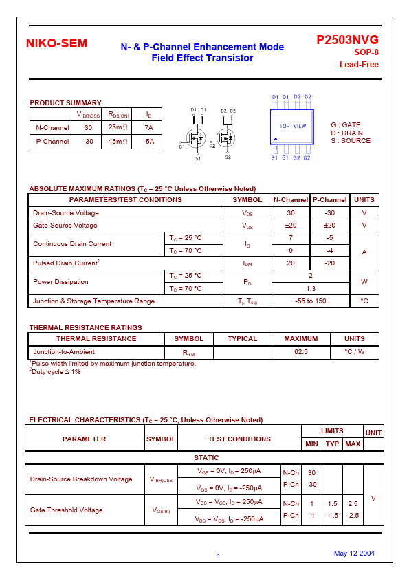
NIKO-SEM N- & P-Channel Enhancement Mode Field Effect Transistor P2503NVG SOP-8 Lead-Free PRODUCT SUMMARY V(BR)DSS RDS(ON) N-Channel 30 25mΩ P-Channel -30 45mΩ ID 7A -5A G.
P2503NVG is N- & P-Channel FET manufactured by NIKO-SEM.
| Manufacturer | Part Number | Description |
|---|---|---|
| P2503NVG | N&P-Channel MOSFET | |
| P2503BDG | N-Channel MOSFET | |
| P2503HEA | MOSFET | |
| P2503HVG | N-Channel MOSFET |
NIKO-SEM N- & P-Channel Enhancement Mode Field Effect Transistor P2503NVG SOP-8 Lead-Free PRODUCT SUMMARY V(BR)DSS RDS(ON) N-Channel 30 25mΩ P-Channel -30 45mΩ ID 7A -5A G.