Click to expand full text
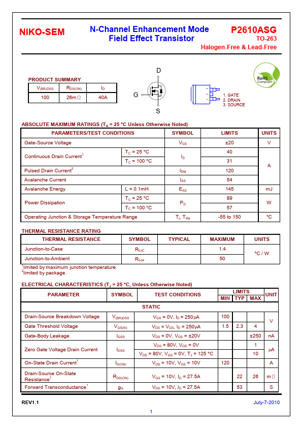
NIKO-SEM
N-Channel Enhancement Mode
P2610ASG
Field Effect Transistor
TO-263
Halogen-Free & Lead-Free
PRODUCT SUMMARY
V(BR)DSS
RDS(ON)
100
26mΩ
ID 40A
D
G S
123
1. GATE 2. DRAIN 3. SOURCE
ABSOLUTE MAXIMUM RATINGS (TA = 25 °C Unless Otherwise Noted)
PARAMETERS/TEST CONDITIONS
SYMBOL
Gate-Source Voltage
Continuous Drain Current1 Pulsed Drain Current2
TC = 25 °C TC = 100 °C
Avalanche Current
Avalanche Energy
L = 0.1mH
Power Dissipation
TC = 25 °C TC = 100 °C
Operating Junction & Storage Temperature Range
VGS ID IDM IAS EAS PD Tj, Tstg
LIMITS ±20 40 31 120 54 145 89 57
-55 to 150
UNITS V
A
mJ W °C
THERMAL RESISTANCE RATING THERMAL RESISTANCE
Junction-to-Case Junction-to-Ambient 1limited by maximum junction temperature. 2limited by package.