74HCT4051-Q100 Description
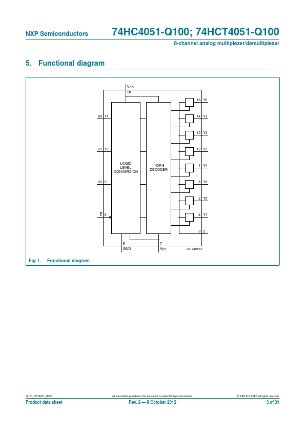
74HCT4051-Q100 is a high-speed Si-gate CMOS device and is pin patible with Low-power Schottky TTL (LSTTL). The device is specified in pliance with JEDEC standard no. 74HCT4051-Q100 is an 8-channel analog multiplexer/demultiplexer with three digital select inputs (S0 to S2), an active-LOW enable input (E), eight independent inputs/outputs (Y0 to Y7) and a mon input/output (Z).
74HCT4051-Q100 Key Features
- Automotive product qualification in accordance with AEC-Q100 (Grade 1)
- Specified from 40 C to +85 C and from 40 C to +125 C
- Wide analog input voltage range from 5 V to +5 V
- Low ON resistance
- 80 (typical) at VCC VEE = 4.5 V
- 70 (typical) at VCC VEE = 6.0 V
- 60 (typical) at VCC VEE = 9.0 V
- Logic level translation: to enable 5 V logic to municate with 5 V analog signals
- ESD protection
- MIL-STD-883, method 3015 exceeds 2000 V
74HCT4051-Q100 Applications
- Automotive product qualification in accordance with AEC-Q100 (Grade 1) Specified from 40 C to +85 C and from 40 C to +125 C
- Wide analog input voltage range from 5 V to +5 V