Datasheet4U Logo Datasheet4U.com

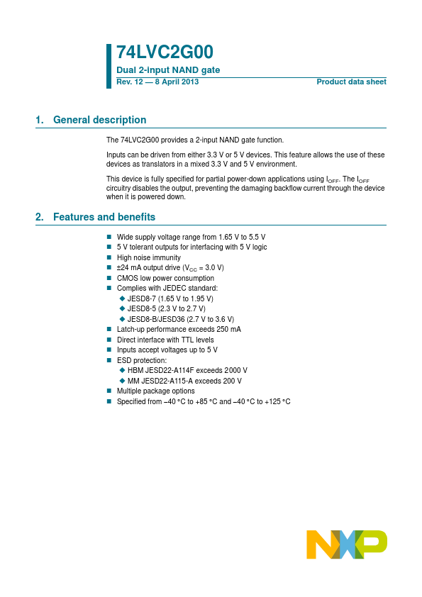
74LVC2G00 - Dual 2-input NAND gate

General Description

The 74LVC2G00 provides a 2-input NAND gate function.

Inputs can be driven from either 3.3 V or 5 V devices.

This feature allows the use of these devices as translators in a mixed 3.3 V and 5 V environment.

Key Features

  • Wide supply voltage range from 1.65 V to 5.5 V.
  • 5 V tolerant outputs for interfacing with 5 V logic.
  • High noise immunity.
  • 24 mA output drive (VCC = 3.0 V).
  • CMOS low power consumption.
  • Complies with JEDEC standard:.
  • JESD8-7 (1.65 V to 1.95 V).
  • JESD8-5 (2.3 V to 2.7 V).
  • JESD8-B/JESD36 (2.7 V to 3.6 V).
  • Latch-up performance exceeds 250 mA.
  • Direct interface with TTL levels.
  • Inputs accept voltages up to 5 V.
  • ESD protection:.
  • HBM.

📥 Download Datasheet

Full PDF Text Transcription (Reference)

The following content is an automatically extracted verbatim text from the original manufacturer datasheet and is provided for reference purposes only.

View original datasheet text
74LVC2G00 Dual 2-input NAND gate Rev. 12 — 8 April 2013 Product data sheet 1. General description The 74LVC2G00 provides a 2-input NAND gate function. Inputs can be driven from either 3.3 V or 5 V devices. This feature allows the use of these devices as translators in a mixed 3.3 V and 5 V environment. This device is fully specified for partial power-down applications using IOFF. The IOFF circuitry disables the output, preventing the damaging backflow current through the device when it is powered down. 2. Features and benefits  Wide supply voltage range from 1.65 V to 5.5 V  5 V tolerant outputs for interfacing with 5 V logic  High noise immunity  24 mA output drive (VCC = 3.0 V)  CMOS low power consumption  Complies with JEDEC standard:  JESD8-7 (1.65 V to 1.95 V)  JESD8-5 (2.