54ACT377 Overview
Key Specifications
Operating Voltage: 5 V
Max Voltage (typical range): 5.5 V
Min Voltage (typical range): 4.5 V
Clock Edge Trigger: Positive Edge
Description
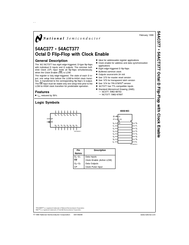
The ’AC/’ACT377 has eight edge-triggered, D-type flip-flops with individual D inputs and Q outputs. The common buffered Clock (CP) input loads all flip-flops simultaneously, when the Clock Enable (CE) is LOW.