54F648 Overview
Description
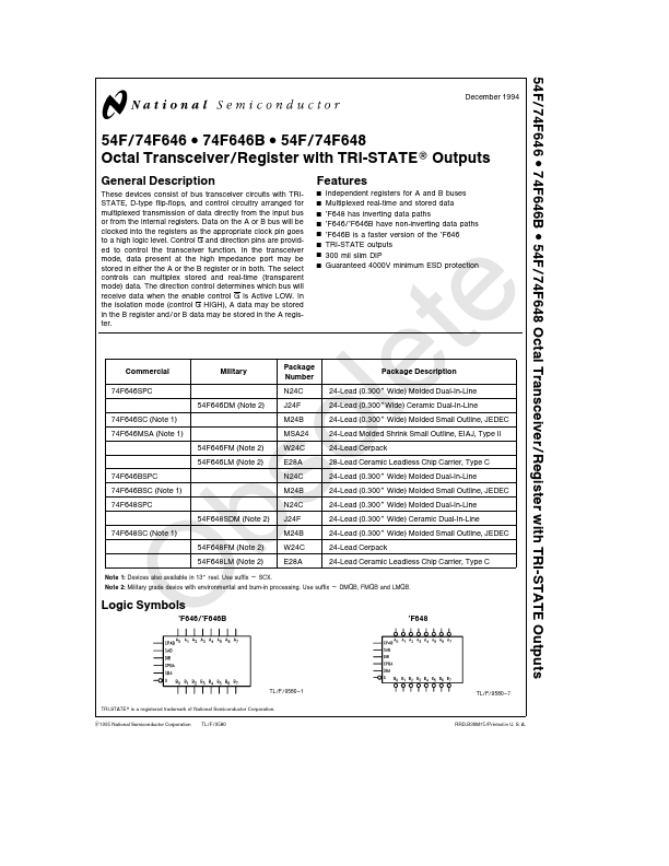
These devices consist of bus transceiver circuits with TRISTATE D-type flip-flops and control circuitry arranged for multiplexed transmission of data directly from the input bus or from the internal registers Data on the A or B bus will be clocked into the registers as the appropriate clock pin goes to a high logic level Control G and direction pins are provided to control the transceiver function In the transceiver mode data present at the high impedance port may be stored in either the A or the B register or in both The select controls can multiplex stored and real-time (transparent mode) data The direction control determines which bus will receive data when the enable control G is Active LOW In the isolation mode (control G HIGH) A data may be stored in the B register and or B data may be stored in the A register.
Key Features
- 74F646MSA (Note
- 74F646BSPC 74F646BSC (Note
- 74F648SPC 74F648SC (Note
- Military 54F646DM (Note
- 54F646FM (Note