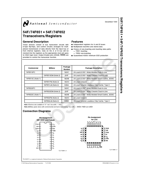
Description
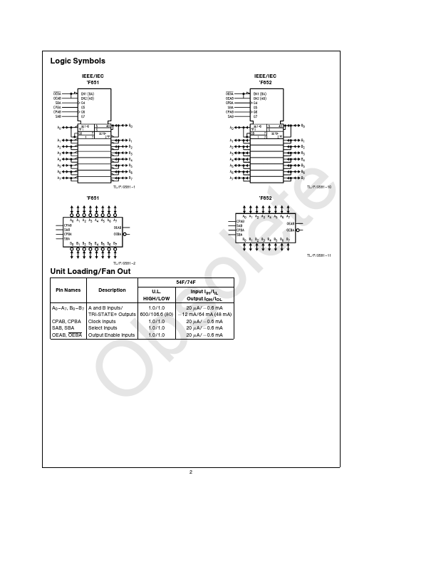
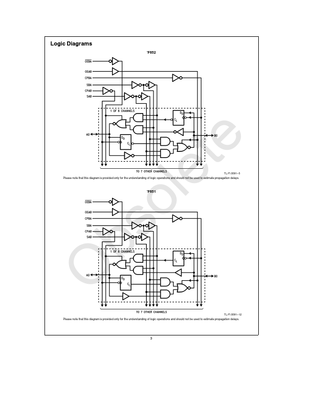
These devices consist of bus transceiver circuits with D-type flip-flops and control circuitry arranged for multiplexed transmission of data directly from the input bus or from internal registers Data on the A or B bus will be clocked into the registers as the appropriate clock pin goes to HIGH logic level Output Enable pins (OEAB OEBA) are provided to control the transceiver function
Features
- Y Independent registers for A and B buses Y Multiplexed real-time and stored data Y Choice of non-inverting and inverting data paths
’F651 inverting ’F652 non-inverting Y Guaranteed 4000V minimum ESD protection
Commercial 74F651SPC 74F651SC (Note 1)
74F652SPC 74F652SC (Note 1)
Military
54F651SDM (Note 2)
54F651FM (Note 2) 54F651LM (Note 2)
54F652SDM (Note 2)
54F652FM (Note 2) 54F652LM (Note 2)
Package Number
N24C J24F M24B W24C E28A N24C J24F M24B W24C E28A
Package.
 54F651-NationalSemiconductor.pdf