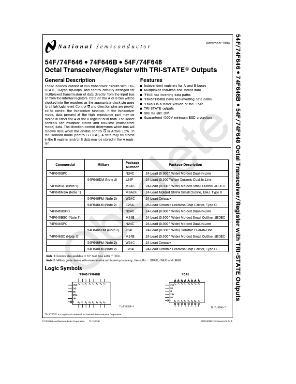
Description
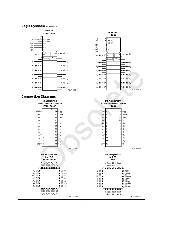
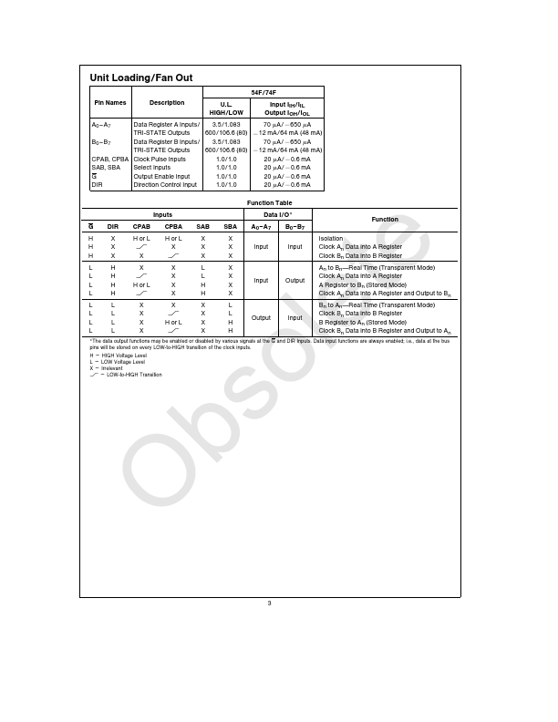
These devices consist of bus transceiver circuits with TRISTATE D-type flip-flops and control circuitry arranged for multiplexed transmission of data directly from the input bus or from the internal registers Data on the A or B bus will be clocked into the registers as the appropriate clock pin goes to a high logic level Control G and direction pins are provided to control the transceiver function In the transceiver mode data present at the high impedance port may be stored in either the A or th
Features
- Y Independent registers for A and B buses Y Multiplexed real-time and stored data Y ’F648 has inverting data paths Y ’F646 ’F646B have non-inverting data paths Y ’F646B is a faster version of the ’F646 Y TRI-STATE outputs Y 300 mil slim DIP Y Guaranteed 4000V minimum ESD protection
Commercial 74F646SPC
74F646SC (Note 1) 74F646MSA (Note 1)
74F646BSPC 74F646BSC (Note 1) 74F648SPC
74F648SC (Note 1)
Military 54F646DM (Note 2)
54F646FM (Note 2) 54F646LM (Note 2)
54F648SDM (Note 2) 54F648FM (Note 2).
 54F646-NationalSemiconductor.pdf