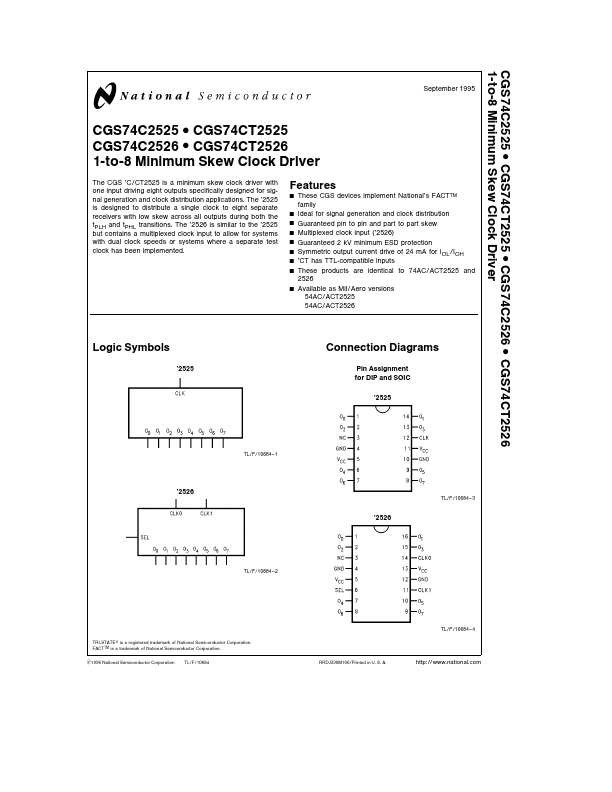
On the multiplexed clock device the SEL pin is used to determine which CLKn input will have an active effect on the outputs of the circuit When SEL e 1 the CLK1 input is selected and when SEL e 0 the CLK0 input is selected The non-selected CLKn input will not have any effect on the logical output le
Key Features
Y Y Y Y Y Y Y Y
Y
These CGS devices implement National’s FACTTM family Ideal for signal generation and clock distribution Guaranteed pin to pin and part to part skew Multiplexed clock input (’2526) Guaranteed 2 kV minimum ESD protection Symmetric output current drive of 24 mA for IOL IOH ’CT has TTL-compatible inputs These products are identical to 74AC ACT2525 and 2526 Available as Mil Aero versions 54AC ACT2525 54AC ACT2526
Logic Symbols
’2525
Connection Diagrams
Pin Assignment for DIP and.
Full PDF Text Transcription for 74C2526 (Reference)
Note: Below is a high-fidelity text extraction (approx. 800 characters) for
74C2526. For precise diagrams, and layout, please refer to the original PDF.
CGS74C2525 CGS74CT2525 CGS74C2526 CGS74CT2526 1-to-8 Minimum Skew Clock Driver The CGS ’C CT2525 is a minimum skew clock driver with one input driving eight outputs specifically designed for signal generation and clock distribution applications The ’2525 is designed to distribute a single clock to eight separate receivers with low skew across all outputs during both the tPLH and tPHL transitions The ’2526 is similar to the ’2525 but contains a multiplexed clock input to allow for systems with dual clock speeds or systems where a separate test clock has been implemented Features Y Y Y Y Y Y Y Y Y These CGS devices imple
More Datasheets from National Semiconductor (now Texas Instruments)