74LS257B Overview
Key Specifications
Package: PDIP
Mount Type: Through Hole
Pins: 16
Operating Voltage: 5 V
Description
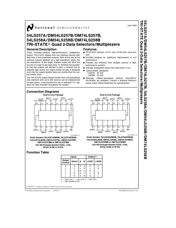
These Schottky-clamped high-performance multiplexers feature TRI-STATE outputs that can interface directly with data lines of bus-organized systems With all but one of the common outputs disabled (at a high impedance state) the low impedance of the single enabled output will drive the bus line to a high or low logic level To minimize the possibility that two outputs will attempt to take a common bus to opposite logic levels the output enable circuitry is designed such that the output disable times are shorter than the output enable times This TRI-STATE output feature means that n-bit (paralleled) data selectors with up to 258 sources can be implemented for data buses It also permits the use of standard TTL registers for data retention throughout the system.
Key Features
- Z L L LX L H L L HX H L L