Description
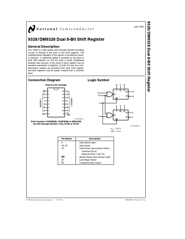
The ’9328 is a high speed serial storage element providing 16 bits of storage in the form of two 8-bit registers The multifunctional capability of this device is provided by several features 1) additional gating is provided at the input to both shift registers so that the input is easily multiplexed between two sources 2) the clock of each register may be provided separately or together 3) both the true and plementary outputs are provided from each 8-bit register and both registers may be master cleared from a mon input Connection Diagram Dual-In-Line Package Logic Symbol TL F 9793 - 1 Order Number 9328DMQB 9328FMQB or DM9328N See NS Package Number J16A N16E or W16A TL F 9793 - 2 VCC e Pin 16 GND e Pin 8 Pin Names S D0 D1 CP Description Data Select Input Data Inputs Clock Pulse Input (Active HIGH) mon (Pin 9) Separate (Pins 7 and 10) Master Reset Input (Active LOW) Last Stage Output plementary Output MR Q7 Q7 C1995 National Semiconductor Corporation TL F 9793 RRD-B30M115 Printed in U S A If Military Aerospace specified devices are required please contact the National Semiconductor Sales Office Distributors for availability and specifications Supply Voltage 7V Input Voltage 5 5V Operating Free Air Temperature Range b 55 C to a 125 C Military mercial 0 C to a 70 C Storage Temperature Range b 65 C to a 150 C Note The ‘‘ Remended Operating Conditions Symbol VCC VIH VIL IOH IOL TA ts (H) ts (L) th (H) th (L) tw (H) tw (L) tw (L) tw (L) trec Parameter Min Supply Voltage High Level Input Voltage Low Level Input Voltage High Level Output Current Low Level Output Current Free Air Operating Temperature Setup Time HIGH or LOW Dn to CP Hold Time HIGH or LOW Dn to CP Clock Pulse Width HIGH or LOW MR Pulse Width with CP HIGH MR Pulse Width with CP LOW Recovery Time MR to CP b 55 Military Nom 5 Max 55 Min 4 75 2 08 b0 4 mercial Nom 5 Max 5 25 Units V V 08 b0 4 45 2 V mA mA C ns ns ns ns ns ns 16 125 0 20 20 0 0 25 25 30 40 33 16 70 20 20 0 0 25 25 30 40 33 Over Remended Operating Free Air Temperature Range (Unless Otherwise Noted) Symbol VI VOH VOL II IIH Parameter Input Clamp Voltage High Level Output Voltage Low Level Output Voltage Input Current Max Input Voltage Conditions VCC e Min II e b12 mA VCC e Min IOH e Max VIL e Max VCC e Min IOL e Max VIH e Min VCC e Max VI e 5 5V VCC e Max VI e 2 4V MR Dn Inputs CP Inputs S Inputs CP () Inputs IIL Low Level Input Current VCC e Max VI e 0 4V MR Dn Inputs CP Inputs S Inputs CP () Input 24 34 02 04 1 40 60 80 120 b1 6 b2 4 b3 2 b4 8 Min Typ (Note 1) Max b1 5 Units V V V mA High Level Input Current mA mA 2 Over Remended Operating Free Air Temperature Range (Unless Otherwise Noted) (Continued) Symbol IOS ICC Parameter Short Circuit Output Current Supply Current Conditions VCC e Max (Note 2) VCC e Max MIL M Min b 20 b 20 Typ (Note 1) Max b 70 b 70 Units mA mA 77 Note 1 All typicals are at VCC e 5V TA e 25 C Note 2 Not more than one output should be shorted at a time Switching Characteristics VCC e a 5 0V TA e a 25 C (See Section 1 for waveforms and load configurations) Symbol Parameter Min fmax tPLH tPHL tPHL Maximum Shift Right Frequency Propagation Delay CP to Q7 or Q7 Propagation Delay MR to Q7 20 20 35 50 CL e 15 pF RL e 400X Max MHz ns ns Units.
Key Features
- 1) additional gating is provided at the input to both shift registers so that the input is easily multiplexed between two sources
- the clock of each register may be provided separately or together