• Part: CD4093BC
  • Description: Quad 2-Input NAND Schmitt Trigger
  • Manufacturer: National Semiconductor
  • Size: 157.17 KB
Download CD4093BC Datasheet PDF
National Semiconductor
CD4093BC
CD4093BC is Quad 2-Input NAND Schmitt Trigger manufactured by National Semiconductor.
Description 
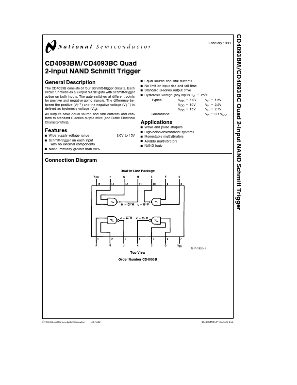
The CD4093B consists of four Schmitt-trigger circuits Each circuit functions as a 2-input NAND gate with Schmitt-trigger action on both inputs The gate switches at different points for positive and negative-going signals The difference between the positive (VT a ) and the negative voltage (VTb) is defined as hysteresis voltage (VH) All outputs have equal source and sink currents and conform to standard B-series output drive (see Static Electrical Characteristics) Equal source and sink currents No limit on input rise and fall time Standard B-series output drive Hysteresis voltage (any input) TA e 25 C VH e 1 5V Typical VDD e 5 0V VDD e 10V VH e 2 2V VDD e 15V VH e 2 7V Guaranteed VH e 0 1 VDD Applications Y Y Y Y Y Features Wide supply voltage range Schmitt-trigger on each input with no external ponents Noise immunity greater than 50% 3 0V to 15V Wave and pulse shapers High-noise-environment systems Monostable multivibrators Astable multivibrators NAND logic Connection Diagram Dual-In-Line Package TL F 5982 - 1 Top View Order Number CD4093B C1995 National Semiconductor Corporation TL F 5982 RRD-B30M105 Printed in U S A Absolute Maximum Ratings (Notes 1 2) If Military Aerospace specified devices are required please contact the National Semiconductor Sales Office Distributors for availability and specifications DC Supply Voltage (VDD) Input Voltage (VIN) Storage Temperature Range (TS) Power Dissipation (PD) Dual-In-Line Small Outline Lead Temperature (TL) (Soldering 10 seconds) b 0 5 to a 18 VDC b 0 5 to VDD a 0 5 VDC b 65 C to a 150 C Remended Operating Conditions (Note 2) DC Supply Voltage (VDD) Input Voltage (VIN) Operating Temperature Range (TA) CD4093BM CD4093BC 3 to 15 VDC 0 to VDD VDC b 55 C to a 125 C b 40 C to a 85 C 700 m W 500 m W 260 C DC Electrical Characteristics CD4093BM (Note 2) Symbol IDD Parameter Quiescent Device Current Low Level Output Voltage Conditions VDD e 5V VDD e 10V VDD e 15V VIN e VDD l IOl k 1 m A...