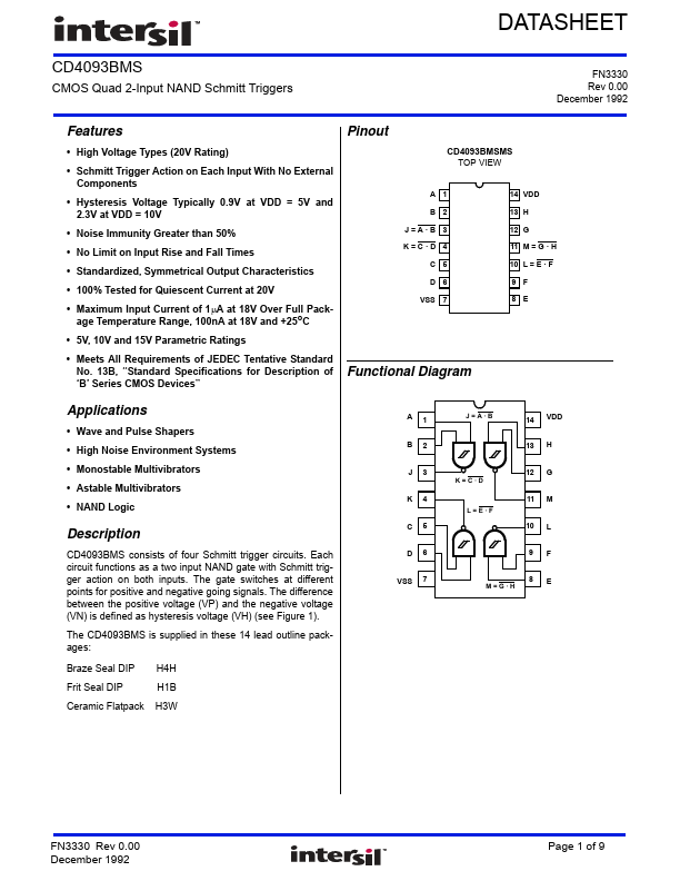
CD4093BMS
Description
CD4093BMS consists of four Schmitt trigger circuits. Each circuit functions as a two input NAND gate with Schmitt trigger action on both inputs.
Key Features
- High Voltage Types (20V Rating)
- Hysteresis Voltage Typically 0.9V at VDD = 5V and 2.3V at VDD = 10V
- Noise Immunity Greater than 50%
- No Limit on Input Rise and Fall Times
- Standardized, Symmetrical Output Characteristics
- 100% Tested for Quiescent Current at 20V
- Maximum Input Current of 1µA at 18V Over Full Package Temperature Range, 100nA at 18V and +25oC
- 5V, 10V and 15V Parametric Ratings
- Meets All Requirements of JEDEC Tentative Standard No. 13B, “Standard Specifications for Description of ‘B’ Series CMOS Devices” A 1 B 2 J=A
- D 4 C 5 D 6 VSS 7 14 VDD 13 H 12 G 11 M = G