Datasheet4U Logo Datasheet4U.com

DM54LS109A - Dual Positive-Edge-Triggered J-K Flip-Flops with Preset/ Clear/ and Complementary Outputs

General Description

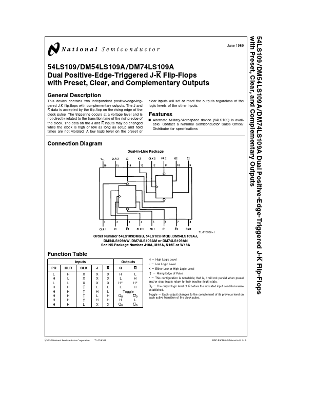
This device contains two independent positive-edge-triggered J-K flip-flops with complementary outputs The J and K data is accepted by the flip-flop on the rising edge of the clock pulse The triggering occurs at a voltage level and is not directly related to the transition time of the rising edge of

Key Features

  • Y Alternate Military Aerospace device (54LS109) is available Contact a National Semiconductor Sales Office Distributor for specifications Connection Diagram Dual-In-Line Package TL F 6368.
  • 1 Order Number 54LS109DMQB 54LS109FMQB DM54LS109AJ DM54LS109AW DM74LS109AM or DM74LS109AN See NS Package Number J16A M16A N16E or W16A Function Table Inputs PR L H L H H H H H CLR H L L H H H H H CLK X X X J X X X L H L H X K X X X L L H H X Outputs Q H L H L Q H e High Logic Level L e Low Logic.

📥 Download Datasheet

Full PDF Text Transcription (Reference)

The following content is an automatically extracted verbatim text from the original manufacturer datasheet and is provided for reference purposes only.

View original datasheet text
54LS109 DM54LS109A DM74LS109A Dual Positive-Edge-Triggered J-K Flip-Flops with Preset Clear and Complementary Outputs June 1989 54LS109 DM54LS109A DM74LS109A Dual Positive-Edge-Triggered J-K Flip-Flops with Preset Clear and Complementary Outputs General Description This device contains two independent positive-edge-triggered J-K flip-flops with complementary outputs The J and K data is accepted by the flip-flop on the rising edge of the clock pulse The triggering occurs at a voltage level and is not directly related to the transition time of the rising edge of the clock The data on the J and K inputs may be changed while the clock is high or low as long as setup and hold times are not violated A low logic level on the preset or clear inputs will set or reset the outputs regardless of the