Datasheet Summary
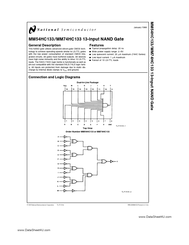
MM54HC133 MM74HC133 13-Input NAND Gate
January 1988
MM54HC133 MM74HC133 13-Input NAND Gate
General Description
This NAND gate utilizes advanced silicon-gate CMOS technology to achieve operating speeds similar to LS-TTL gates with the low power consumption of standard CMOS integrated circuits All gates have buffered outputs All devices have high noise immunity and the ability to drive 10 LS-TTL loads The 54HC 74HC logic family is functionally as well as pin-out patible with the standard 54LS 74LS logic family All inputs are protected from damage due to static discharge by internal diode clamps to VCC and ground
Features
Y Y Y Y Y
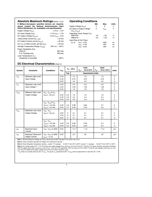
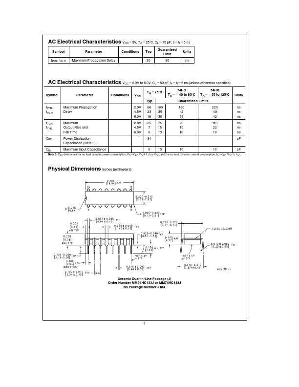
Typical propagation delay 20 ns Wide power supply...