NJG1515AVB2 Datasheet Text
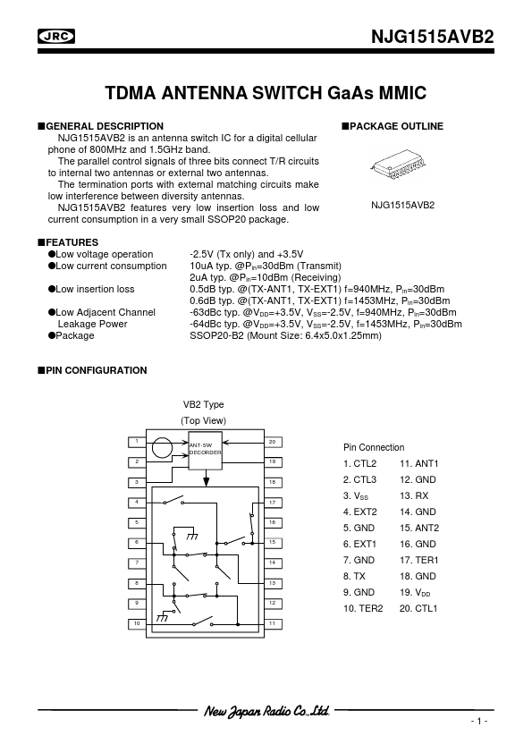
NJG1515AVB2 TDMA ANTENNA SWITCH GaAs MMIC n GENERAL DESCRIPTION NJG1515AVB2 is an antenna switch IC for a digital cellular phone of 800MHz and 1.5GHz band. The parallel control signals of three bits connect T/R circuits to internal two antennas or external two antennas. The termination ports with external matching circuits make low interference between diversity antennas. NJG1515AVB2 Features very low insertion loss and low current consumption in a very small SSOP20 package. n Features lLow voltage operation lLow current consumption lLow insertion loss lLow Adjacent Channel Leakage Power lPackage n PACKAGE OUTLINE
NJG1515AVB2
-2.5V (Tx only) and +3.5V 10uA typ. @Pin=30dBm (Transmit) 2uA typ. @Pin=10dBm (Receiving) 0.5dB typ. @(TX-ANT1, TX-EXT1) f=940MHz, Pin=30dBm 0.6dB typ. @(TX-ANT1, TX-EXT1) f=1453MHz, Pin=30dBm -63dBc typ. @VDD=+3.5V, VSS=-2.5V, f=940MHz, Pin=30dBm -64dBc typ. @VDD=+3.5V, VSS=-2.5V, f=1453MHz, Pin=30dBm SSOP20-B2 (Mount Size: 6.4x5.0x1.25mm) n PIN CONFIGURATION
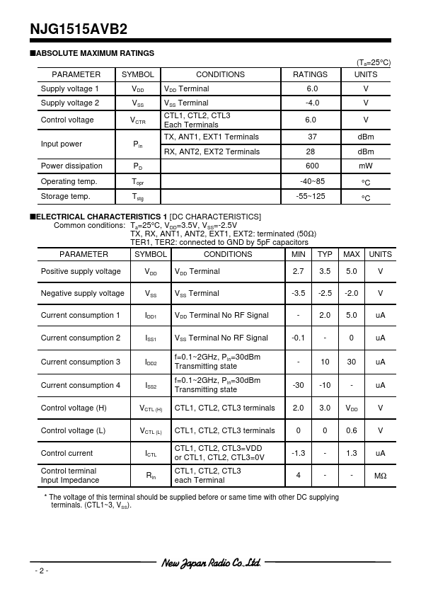
VB2 Type (Top View)
1 ANT-SW DECORDER 20
Pin Connection
2
19
1. CTL2 2. CTL3 3. VSS 4. EXT2 5. GND 6. EXT1 7. GND 8. TX 9. GND 10. TER2
11. ANT1 12. GND 13. RX 14. GND 15. ANT2 16. GND 17. TER1 18. GND 19. VDD 20. CTL1
3
18
4
17
5
16
6
15
7
14
8
13
9
12
10
11
-1-
NJG1515AVB2...