25N60N
25N60N is N-Channel MOSFET manufactured by onsemi.
MOSFET
- N-Channel, SUPREMOS
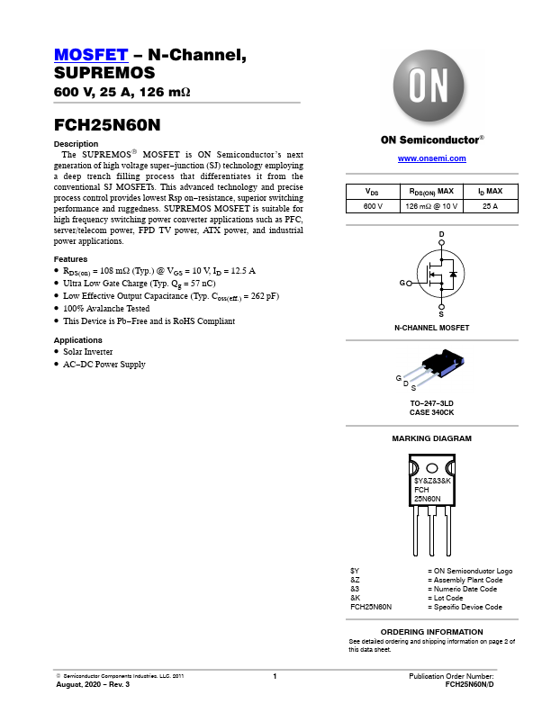
600 V, 25 A, 126 mW
FCH25N60N
Description The SUPREMOS® MOSFET is ON Semiconductor’s next generation of high voltage super- junction (SJ) technology employing a deep trench filling process that differentiates it from the conventional SJ MOSFETs. This advanced technology and precise process control provides lowest Rsp on- resistance, superior switching performance and ruggedness. SUPREMOS MOSFET is suitable for high frequency switching power converter applications such as PFC, server/tele power, FPD TV power, ATX power, and industrial power applications.
Features
- RDS(on) = 108 mW (Typ.) @ VGS = 10 V, ID = 12.5 A
- Ultra Low Gate Charge (Typ. Qg = 57 nC)
- Low...