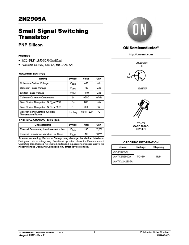
2N2905A
Features
- MIL- PRF- 19500/290 Qualified
- Available as JAN, JANTX, and JANTXV
MAXIMUM RATINGS
Rating Collector
- Emitter Voltage Collector
- Base Voltage Emitter
- Base Voltage Collector Current
- Continuous Total Device Dissipation @ TA = 25°C Total Device Dissipation @ TC = 25°C Operating and Storage Junction Temperature Range
Symbol Value
VCEO
- 60
VCBO
- 60
VEBO IC
- 5.0
- 600
PT 800
PT 3.0
TJ, Tstg
- 65 to +200
Unit Vdc Vdc Vdc m Adc m W W °C
THERMAL CHARACTERISTICS
Characteristic
Symbol
Max
Unit
Thermal Resistance, Junction- to- Ambient Rq JA
195 °C/W
Thermal Resistance, Junction- to- Case
Rq JC
50 °C/W
Stresses exceeding Maximum Ratings may damage the device. Maximum Ratings are stress ratings only. Functional operation above the Remended Operating Conditions is not implied. Extended exposure to stresses above the Remended Operating Conditions may affect device...