The following content is an automatically extracted verbatim text
from the original manufacturer datasheet and is provided for reference purposes only.
View original datasheet text
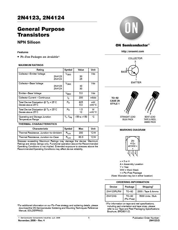
2N4123, 2N4124
General Purpose Transistors
NPN Silicon
Features
• Pb−Free Packages are Available*
MAXIMUM RATINGS
Rating Collector−Emitter Voltage
Symbol Value
Unit
VCEO
Vdc
2N4123
30
2N4124
25
Collector−Base Voltage
VCBO
Vdc
2N4123
40
2N4124
30
Emitter−Base Voltage Collector Current − Continuous Total Device Dissipation @ TA = 25°C Derate above 25°C
VEBO IC PD
5.0
Vdc
200
mAdc
625
mW
5.0
mW/°C
Total Device Dissipation @ TC = 25°C
PD
1.5
W
Derate above 25°C
12
mW/°C
Operating and Storage Junction Temperature Range
TJ, Tstg −55 to +150 °C
THERMAL CHARACTERISTICS
Characteristic
Symbol
Max
Unit
Thermal Resistance, Junction−to−Ambient RqJA
200
°C/W
Thermal Resistance, Junction−to−Case
RqJC
83.
 2N4123 Datasheet