2N5038
Key Features
- ăHigh Speed - tf = 0.5 ms (Max)
- ăHigh Current - IC(max) = 30 Amps
- ăLow Saturation - VCE(sat) = 2.5 V (Max) @ IC = 20 Amps
- ăPb-Free Package is Available*
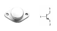
Representative 2N5038 image (package may vary by manufacturer)
Representative 2N5038 image (package may vary by manufacturer)
| Part Number | Manufacturer | Description |
|---|---|---|
| 2N5038 | Seme LAB | Bipolar NPN Device |
| 2N5038 | Motorola Semiconductor | NPN SILICON TRANSISTORS |
| 2N5038 | NTE Electronics | Silicon NPN Transistor |
| 2N5038 | Inchange Semiconductor | NPN Transistor |
| 2N5038 | Semicoa Semiconductor | Silicon NPN Transistor |
| 2N5038 | VPT Components | NPN High Power Silicon Transistor |
| 2N5031 | Motorola Semiconductor | HIGH FREQUENCY TRANSISTOR |
| 2N5039 | GE | SILICON N-P-N PLANAR TRANSISTORS |
| 2N5034 | RCA | Power Transistors |
| 2N5035 | RCA | Power Transistors |