2N5087 Overview
Key Features
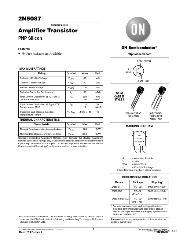
- Pb-Free Packages are Available* 3 COLLECTOR
| Part | 2N5087 |
|---|---|
| Description | Amplifier Transistor |
| Category | Transistor |
| Manufacturer | onsemi |
| Size | 158.91 KB |
| Part Number | Manufacturer | Description |
|---|---|---|
| 2N5087 | Motorola Semiconductor | Amplifier Transistor |
| 2N5087 | NXP Semiconductors | PNP general purpose transistor |
| 2N5087 | Fairchild Semiconductor | PNP General Purpose Amplifier |
| 2N5087 | SEMTECH | PNP Silicon Epitaxial Planar Transistor |
| 2N5087 | Taitron Components | Small Signal Low Noise Transistors |