2N5550
2N5550 is Amplifier Transistor manufactured by onsemi.
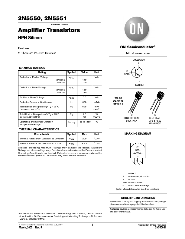
2N5550, 2N5551
Preferred Device
Amplifier Transistors
NPN Silicon
Features
- These are Pb- Free Devices-
MAXIMUM RATINGS
Rating Collector
- Emitter Voltage
Symbol
2N5550 2N5551
VCEO
Value
140 160
Unit Vdc
Collector
- Base Voltage
VCBO
Vdc
2N5551
Emitter
- Base Voltage Collector Current
- Continuous Total Device Dissipation @ TA = 25°C Derate above 25°C
VEBO IC PD
Vdc
600 m Adc
625 m W
5.0 m W/°C
Total Device Dissipation @ TC = 25°C Derate above 25°C
12 m...