The following content is an automatically extracted verbatim text
from the original manufacturer datasheet and is provided for reference purposes only.
View original datasheet text
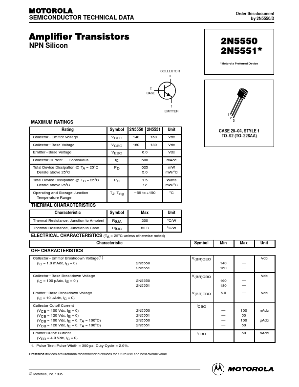
MOTOROLA
SEMICONDUCTOR TECHNICAL DATA
Order this document by 2N5550/D
Amplifier Transistors
NPN Silicon
COLLECTOR 3
2 BASE
1 EMITTER
MAXIMUM RATINGS Rating
Collector – Emitter Voltage
Collector – Base Voltage
Emitter – Base Voltage
Collector Current — Continuous
Total Device Dissipation @ TA = 25°C Derate above 25°C
Total Device Dissipation @ TC = 25°C Derate above 25°C
Operating and Storage Junction Temperature Range
Symbol VCEO VCBO VEBO
IC PD
PD
TJ, Tstg
2N5550 2N5551
140
160
160
180
6.0
600
625 5.0
1.5 12
– 55 to +150
Unit Vdc Vdc Vdc mAdc mW mW/°C Watts mW/°C °C
THERMAL CHARACTERISTICS
Characteristic
Symbol
Max
Unit
Thermal Resistance, Junction to Ambient RqJA
200
°C/W
Thermal Resistance, Junction to Case
RqJC
83.