2N5657 Description
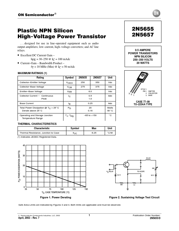
ON Semiconductor ) Plastic NPN Silicon High-Voltage Power Transistor . designed for use in line operated equipment such as audio output amplifiers; low current, high voltage converters;.
2N5657 is POWER TRANSISTORS manufactured by onsemi.
| Manufacturer | Part Number | Description |
|---|---|---|
| 2N5657 | SILICON NPN TRANSISTOR | |
| 2N5657 | POWER TRANSISTORS | |
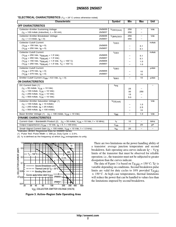
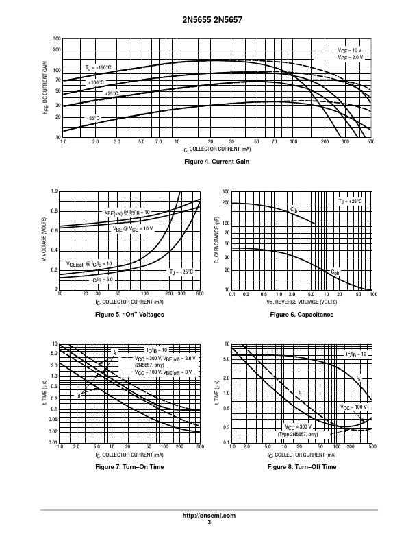
| 2N5657 | (2N5655 - 2N5657) Silicon NPN Power Transistors |
ON Semiconductor ) Plastic NPN Silicon High-Voltage Power Transistor . designed for use in line operated equipment such as audio output amplifiers; low current, high voltage converters;.