ATP112
Features
- ON-resistance RDS(on)1=33mΩ(typ.)
- 4V drive
- Protection diode in
- Input Capacitance Ciss=1450p F(typ.)
- Halogen free pliance
Specifications
Absolute Maximum Ratings at Ta=25°C
Parameter
Symbol
Drain-to-Source Voltage Gate-to-Source Voltage Drain Current (DC) Drain Current (PW≤10μs) Allowable Power Dissipation Channel Temperature
VDSS VGSS ID IDP PD Tch
Storage Temperature
Tstg
Avalanche Energy (Single Pulse)
- 1
Avalanche Current
- 2
Note :- 1 VDD=--10V, L=500μH, IAV=--13A
- 2 L≤500μH, Single pulse
Conditions
PW≤10μs, duty cycle≤1% Tc=25°C
Ratings --60 ±20 --25 --75 40 150
--55 to +150 50
--13
Unit V V A A W °C °C m J A
Stresses exceeding Maximum Ratings may damage the device. Maximum Ratings are stress ratings only. Functional operation above the Remended Operating Conditions is not implied. Extended exposure to stresses above the Remended Operating Conditions may affect device reliability.
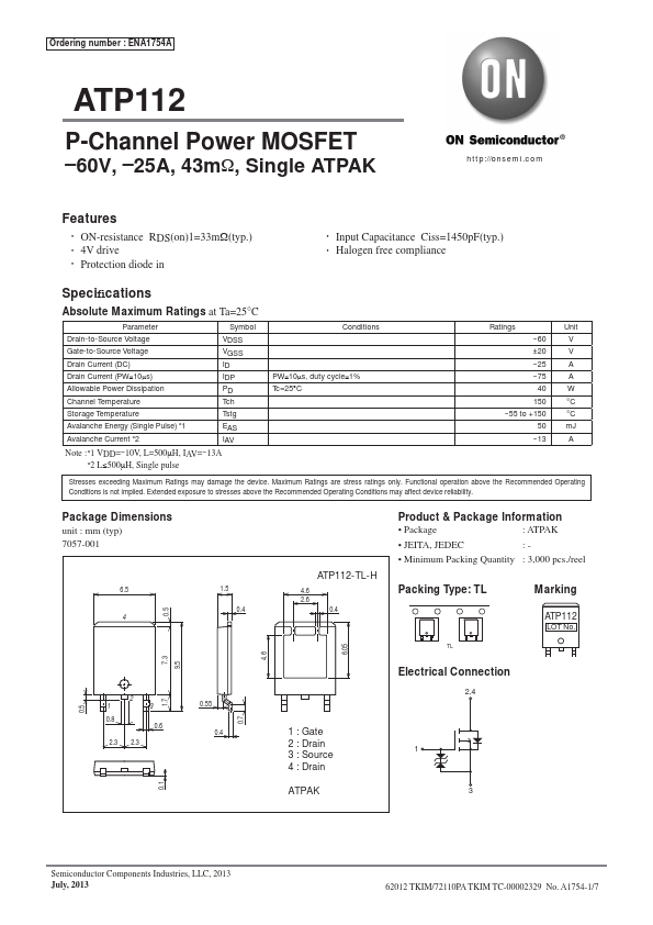
Package Dimensions unit : mm (typ) 7057-001
1.5...