FDC6301N
FDC6301N is Dual N-Channel Digital FET manufactured by onsemi.
Description
These dual N- Channel logic level enhancement mode field effect transistors are produced using onsemi’s proprietary, high cell density, DMOS technology. This very high density process is especially tailored to minimize on- state resistance. This device has been designed especially for low voltage applications as a replacement for digital transistors. Since bias resistors are not required, these N- Channel FET’s can replace several digital transistors, with a variety of bias resistors.
Features
- 25 V, 0.22 A Continuous, 0.5 A Peak
- RDS(on) = 5 W @ VGS = 2.7 V
- RDS(on) = 4 W @ VGS = 4.5 V
- Very Low Level Gate Drive Requirements Allowing Direct
Operation in 3 V Circuits. VGS(th) < 1.5 V
- Gate- Source Zener for ESD Ruggedness. >6 k V Human Body Model
- This is a Pb- Free and Halide Free Device
DATA SHEET .onsemi.
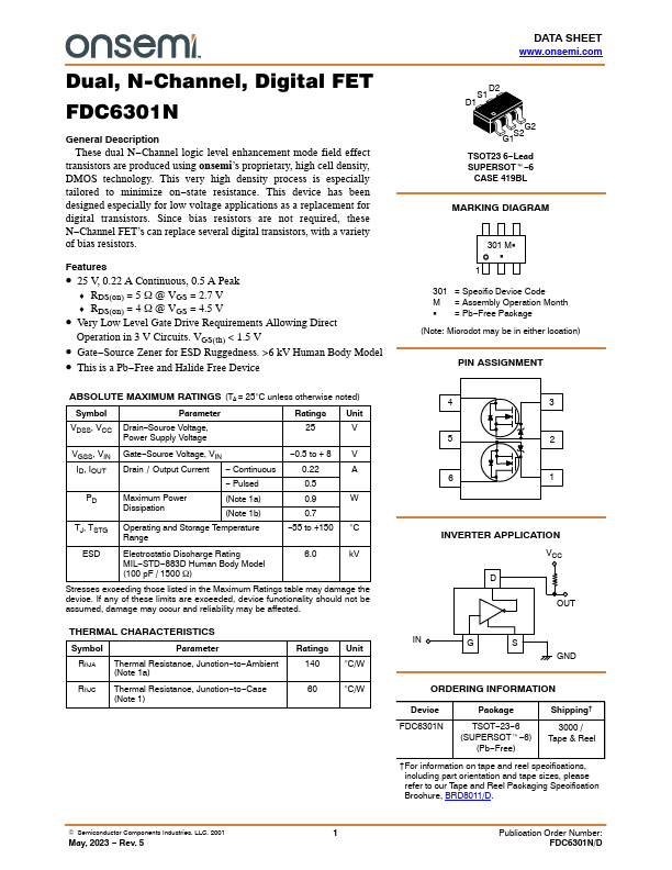
D2 S1 D1
G2 G1S2 TSOT23 6- Lead SUPERSOTt- 6 CASE 419BL
MARKING DIAGRAM
301 MG G
1 301 = Specific Device Code M = Assembly Operation Month G = Pb- Free Package (Note: Microdot may be in either location)
PIN ASSIGNMENT
ABSOLUTE MAXIMUM RATINGS (TA = 25°C unless otherwise noted)
Symbol
Parameter
Ratings Unit
VDSS, VCC Drain- Source Voltage, Power Supply Voltage
VGSS, VIN Gate- Source Voltage, VIN
- 0.5 to + 8 V
ID, IOUT Drain / Output Current
- Continuous
- Pulsed
Maximum Power
Dissipation
(Note 1a) (Note 1b)
TJ, TSTG Operating and Storage Temperature Range
- 55 to +150 °C
Electrostatic Discharge Rating MIL- STD- 883D Human Body Model (100 p F / 1500 W)
6.0 k V
Stresses exceeding those listed in the Maximum Ratings table may damage the device. If any of these limits are exceeded, device functionality should not be assumed, damage may occur and reliability may be...