FDC6304P
FDC6304P is Dual P-Channel MOSFET manufactured by onsemi.
Description
These P-Channel enhancement mode field effect transistor are produced using ON Semiconductor's proprietary, high cell density, DMOS technology. This very high density process is tailored to minimize on-state resistance at low gate drive conditions. This device is designed especially for application in battery power applications such as notebook puters and cellular phones. This device has excellent on-state resistance even at gate drive voltages as low as 2.5 volts.
Features
-25 V, -0.46 A continuous, -1.0 A Peak.
RDS(ON) = 1.5 Ω @ VGS= -2.7 V RDS(ON) = 1.1 Ω @ VGS = -4.5 V.
Very low level gate drive requirements allowing direct operation in 3V circuits. VGS(th) < 1.5 V.
Gate-Source Zener for ESD ruggedness. >6k V Human Body Model.
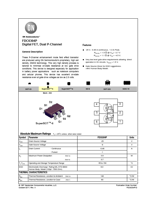
SOT-23
Super SOTTM-6 Mark: .304
Super SOTTM-8
SO-8
SOT-223
SOIC-16
Absolute Maximum Ratings TA = 25o C unless other wise noted
Symbol Parameter
VDSS
Drain-Source Voltage
VGSS
Gate-Source Voltage
Drain Current
- Continuous
- Pulsed
Maximum Power Dissipation
(Note 1a)
(Note 1b)
TJ,TSTG ESD
Operating and Storage Temperature Range
Electrostatic Discharge Rating MIL-STD-883D Human Body Model (100pf / 1500 Ohm)
THERMAL CHARACTERISTICS
RθJA
Thermal Resistance, Junction-to-Ambient (Note...