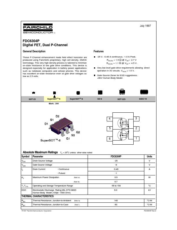
Datasheet4U Logo Datasheet4U.com

FDC6304P - Digital FET/ Dual P-Channel

General Description

These P-Channel enhancement mode field effect transistor are produced using Fairchild's proprietary, high cell density, DMOS technology.

This very high density process is tailored to minimize on-state resistance at low gate drive conditions.

Key Features

  • -25 V, -0.46 A continuous, -1.0 A Peak. RDS(ON) = 1.5 Ω @ VGS= -2.7 V RDS(ON) = 1.1 Ω @ VGS = -4.5 V. Very low level gate drive requirements allowing direct operation in 3V circuits. VGS(th) < 1.5 V. Gate-Source Zener for ESD ruggedness. >6kV Human Body Model. SOT-23 SuperSOTTM-6 Mark: .304 SuperSOTTM-8 SO-8 SOT-223 SOIC-16 4 3 5 2 6 1 Absolute Maximum Ratings Symbol VDSS VGSS ID PD TJ,TSTG ESD Parameter Drain-Source Voltage Gate-Source Voltage Drain Current TA = 25oC unless other.

📥 Download Datasheet

Full PDF Text Transcription (Reference)

The following content is an automatically extracted verbatim text from the original manufacturer datasheet and is provided for reference purposes only.

View original datasheet text
July 1997 FDC6304P Digital FET, Dual P-Channel General Description These P-Channel enhancement mode field effect transistor are produced using Fairchild's proprietary, high cell density, DMOS technology. This very high density process is tailored to minimize on-state resistance at low gate drive conditions. This device is designed especially for application in battery power applications such as notebook computers and cellular phones. This device has excellent on-state resistance even at gate drive voltages as low as 2.5 volts. Features -25 V, -0.46 A continuous, -1.0 A Peak. RDS(ON) = 1.5 Ω @ VGS= -2.7 V RDS(ON) = 1.1 Ω @ VGS = -4.5 V. Very low level gate drive requirements allowing direct operation in 3V circuits. VGS(th) < 1.5 V. Gate-Source Zener for ESD ruggedness.