Datasheet4U Logo Datasheet4U.com

FDC6321C - Dual N & P-Channel Digital FET

Datasheet Summary

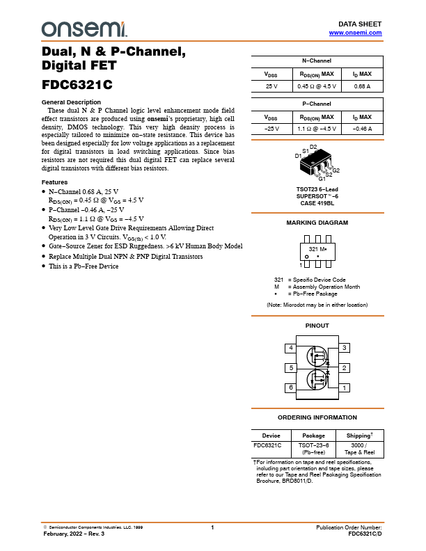
Description

effect transistors are produced using onsemi’s proprietary, high cell density, DMOS technology.

state resistance.

Features

  • N.
  • Channel 0.68 A, 25 V RDS(ON) = 0.45 W @ VGS = 4.5 V.
  • P.
  • Channel.
  • 0.46 A,.
  • 25 V RDS(ON) = 1.1 W @ VGS =.
  • 4.5 V.
  • Very Low Level Gate Drive Requirements Allowing Direct Operation in 3 V Circuits. VGS(th) < 1.0 V.
  • Gate.
  • Source Zener for ESD Ruggedness. >6 kV Human Body Model.
  • Replace Multiple Dual NPN & PNP Digital Transistors.
  • This is a Pb.
  • Free Device DATA SHEET www. onsemi. com VDSS 25 V.

📥 Download Datasheet

Datasheet preview – FDC6321C

Datasheet Details

Part number FDC6321C
Manufacturer ON Semiconductor
File Size 332.77 KB
Description Dual N & P-Channel Digital FET
Datasheet download datasheet FDC6321C Datasheet
Additional preview pages of the FDC6321C datasheet.
Other Datasheets by ON Semiconductor

Full PDF Text Transcription

Click to expand full text
Dual, N & P-Channel, Digital FET FDC6321C General Description These dual N & P Channel logic level enhancement mode field effect transistors are produced using onsemi’s proprietary, high cell density, DMOS technology. This very high density process is especially tailored to minimize on−state resistance. This device has been designed especially for low voltage applications as a replacement for digital transistors in load switching applications. Since bias resistors are not required this dual digital FET can replace several digital transistors with different bias resistors. Features • N−Channel 0.68 A, 25 V RDS(ON) = 0.45 W @ VGS = 4.5 V • P−Channel −0.46 A, −25 V RDS(ON) = 1.1 W @ VGS = −4.5 V • Very Low Level Gate Drive Requirements Allowing Direct Operation in 3 V Circuits. VGS(th) < 1.
Published: |