FDC653N
FDC653N is N-Channel MOSFET manufactured by onsemi.
Description
This N- Channel enhancement mode power field effect transistor is produced using onsemi’s proprietary, high cell density, DMOS technology. This very high density process is tailored to minimize on- state resistance. These devices are particularly suited for low voltage applications in notebook puters, portable phones, PCMICA cards, and other battery powered circuits where fast switching, and low in- line power loss are needed in a very small outline surface mount package.
Features
- 5.0 A, 30 V
RDS(ON) = 0.035 W @ VGS = 10 V RDS(ON) = 0.055 W @ VGS = 4.5 V
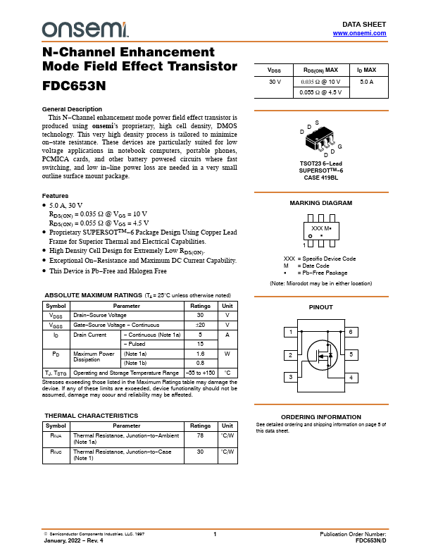
- Proprietary SUPERSOTTM- 6 Package Design Using Copper Lead
Frame for Superior Thermal and Electrical Capabilities.
- High Density Cell Design for Extremely Low RDS(ON).
- Exceptional On- Resistance and Maximum DC Current Capability.
- This Device is Pb- Free and Halogen Free
ABSOLUTE MAXIMUM RATINGS (TA = 25°C unless otherwise noted)
Symbol
Parameter
Ratings Unit
VDSS Drain- Source Voltage
VGSS Gate- Source Voltage
- Continuous
±20
Drain Current
- Continuous (Note 1a)
- Pulsed
Maximum Power (Note 1a)
Dissipation
(Note 1b)
TJ, TSTG Operating and Storage Temperature Range
- 55 to +150 °C
Stresses exceeding those listed in the Maximum Ratings table may damage the device. If any of these limits are exceeded, device functionality should not be assumed, damage may occur and reliability may be affected.
THERMAL CHARACTERISTICS
Symbol
Parameter
Rq JA
Thermal Resistance, Junction- to- Ambient (Note 1a)
Rq JC
Thermal Resistance, Junction- to- Case (Note...