Datasheet4U Logo Datasheet4U.com

FDG313N - N-Channel Digital FET

Description

This N-Channel enhancement mode field effect transistor is produced using Fairchild's proprietary, high cell density, DMOS technology.

This very high density process is especially tailored to minimize on-state resistance.

Features

  • 0.95 A, 25 V. RDS(on) = 0.45 Ω @ VGS = 4.5 V RDS(on) = 0.60 Ω @ VGS = 2.7 V.
  • Low gate charge (1.64 nC typical).
  • Very low level gate drive requirements allowing direct operation in 3V circuits (VGS(th) < 1.5V).
  • Gate-Source Zener for ESD ruggedness (>6kV Human Body Model).
  • Com
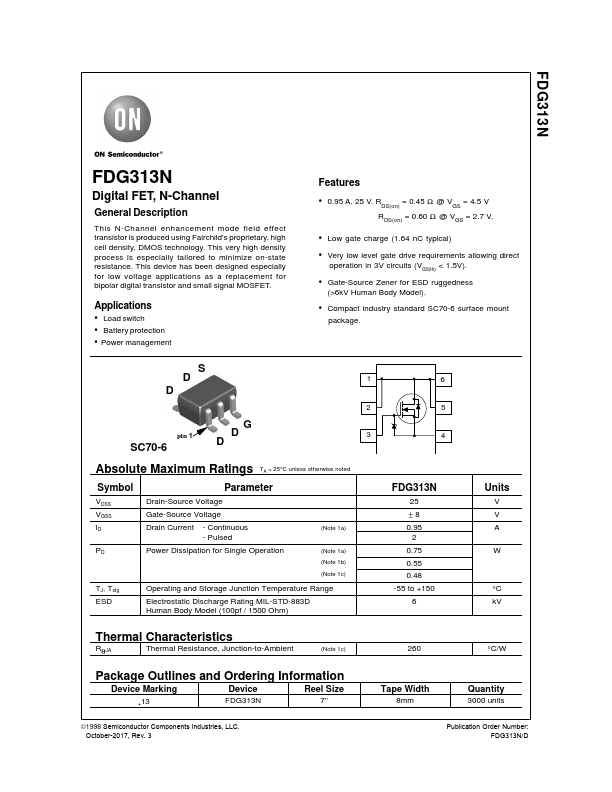
pact industry standard SC70-6 surface mount package. S D 1 D 2 G pin 1 SC70-6 D D 3 Absolute Maximum Ratings TA = 25°C unless otherwise noted Symbol Parameter VDSS.

📥 Download Datasheet

Datasheet preview – FDG313N

Datasheet Details

Part number FDG313N
Manufacturer ON Semiconductor
File Size 171.37 KB
Description N-Channel Digital FET
Datasheet download datasheet FDG313N Datasheet
Additional preview pages of the FDG313N datasheet.
Other Datasheets by ON Semiconductor

Full PDF Text Transcription

Click to expand full text
FDG313N FDG313N Digital FET, N-Channel General Description This N-Channel enhancement mode field effect transistor is produced using Fairchild's proprietary, high cell density, DMOS technology. This very high density process is especially tailored to minimize on-state resistance. This device has been designed especially for low voltage applications as a replacement for bipolar digital transistor and small signal MOSFET. Applications • Load switch • Battery protection • Power management Features • 0.95 A, 25 V. RDS(on) = 0.45 Ω @ VGS = 4.5 V RDS(on) = 0.60 Ω @ VGS = 2.7 V. • Low gate charge (1.64 nC typical) • Very low level gate drive requirements allowing direct operation in 3V circuits (VGS(th) < 1.5V). • Gate-Source Zener for ESD ruggedness (>6kV Human Body Model).
Published: |