FDMD8430
Overview
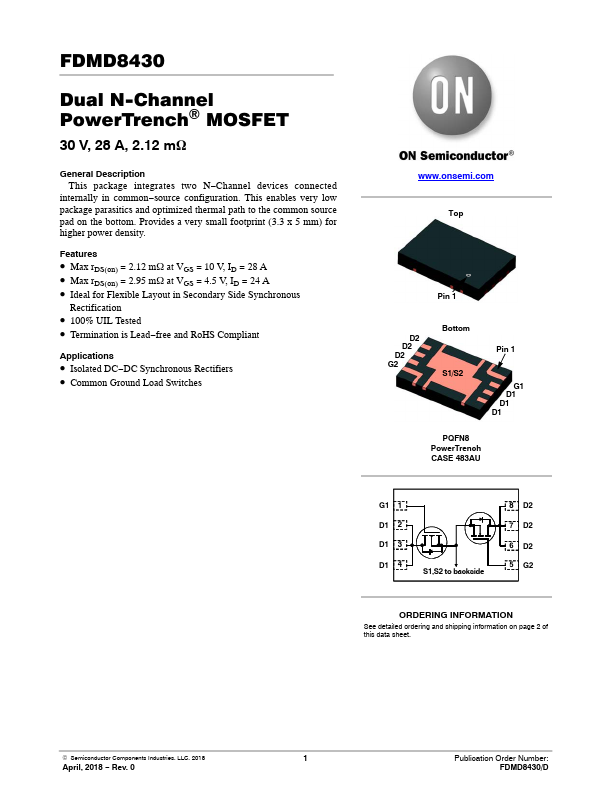
This package integrates two N-Channel devices connected internally in common-source configuration. This enables very low package parasitics and optimized thermal path to the common source pad on the bottom.
- Max rDS(on) = 2.12 mW at VGS = 10 V, ID = 28 A
- Max rDS(on) = 2.95 mW at VGS = 4.5 V, ID = 24 A
- Ideal for Flexible Layout in Secondary Side Synchronous Rectification
- 100% UIL Tested
- Termination is Lead-free and RoHS Compliant