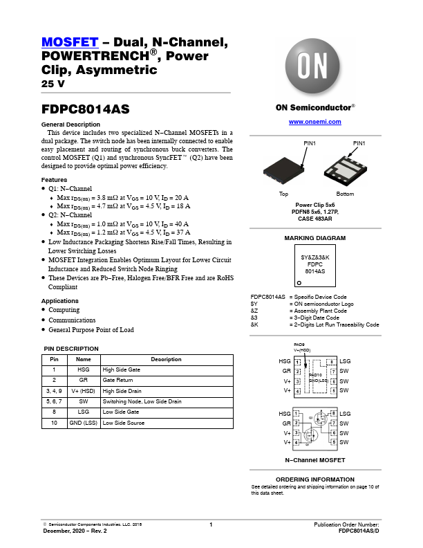
Part number:
FDPC8014AS
Manufacturer:
File Size:
552.25 KB
Description:
Dual n-channel mosfet.
FDPC8014AS Features
* Q1: N
* Channel
* Max rDS(on) = 3.8 mW at VGS = 10 V, ID = 20 A
* Max rDS(on) = 4.7 mW at VGS = 4.5 V, ID = 18 A
* Q2: N
* Channel
* Max rDS(on) = 1.0 mW at VGS = 10 V, ID = 40 A
* Max rDS(on) = 1.2 mW at VGS = 4.5 V, ID = 37 A
FDPC8014AS Datasheet (552.25 KB)
Datasheet Details
FDPC8014AS
552.25 KB
Dual n-channel mosfet.
📁 Related Datasheet
FDPC8014S MOSFET (Fairchild Semiconductor)
FDPC8011S MOSFET (Fairchild Semiconductor)
FDPC8012S MOSFET (Fairchild Semiconductor)
FDPC8013S MOSFET (Fairchild Semiconductor)
FDPC8016S MOSFET (Fairchild Semiconductor)
FDPC8016S Dual N-Channel MOSFET (ON Semiconductor)
FDPC4044 MOSFET (Fairchild Semiconductor)
FDPC4044 N-Channel MOSFET (ON Semiconductor)
FDPC8014AS Distributor