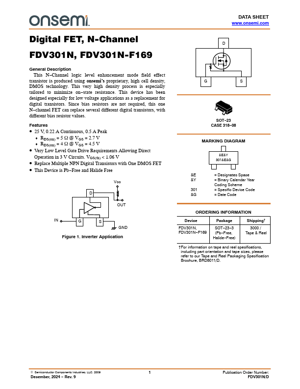
FDV301N Description
This N−Channel logic level enhancement mode field effect transistor is produced using onsemi’s proprietary, high cell density, DMOS technology. This very high density process is especially tailored to minimize on−state resistance. This device has been designed especially for low voltage applications as a replacement for digital transistors.
FDV301N Key Features
- 25 V, 0.22 A Continuous, 0.5 A Peak
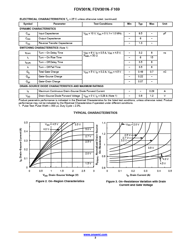
- RDS(on) = 5 W @ VGS = 2.7 V
- RDS(on) = 4 W @ VGS = 4.5 V
- Very Low Level Gate Drive Requirements Allowing Direct
- Replace Multiple NPN Digital Transistors with One DMOS FET
- This Device is Pb-Free and Halide Free
- Rev. 9