GENERAL DESCRIPTION
This device has been designed especially for low voltage applications as a replacement for digital transistors. Since bias resistors are not required, this one N-channel FET can replace several different digital transistors, with different bias resistor values. June 2009 FEATURES
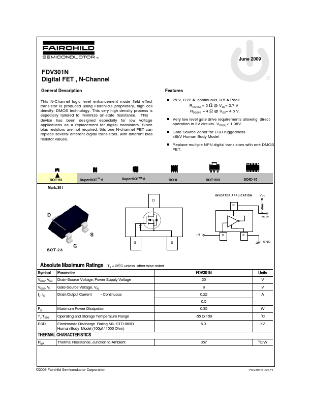
25 V, 0.22 A continuous, 0.5 A Peak. RDS(ON) = 5 Ω @ VGS= 2.7 V RDS(ON) = 4 Ω @ VGS= 4.5 V. Very low level gate drive requirements allowing direct operation in 3V circuits. VGS(th) < 1.06V. Gate-Source Zener for ESD ruggedness. >6kV Human Body Model Replace multiple NPN digital transistors with one DMOS FET. SOT-23 Mark:301 SuperSOTTM-6 SuperSOTTM-8 SO-8 D GS SOT-223 SOIC-16 INVERTER APPLICATION Vcc D OUT IN G S GND ABSOLUTE MAXIMUM RATINGS
TA = 25oC unless other wise noted Symbol Parameter VDSS, VCC Drain-Source Voltage, Power Supply Voltage VGSS, VI Gate-Source Voltage, VIN ID, IO Drain/Output Current - Continuous PD TJ,TSTG ESD Maximum Power Dissipation Operating and Storage Temperature... Fairchild Semiconductor