FDV302P
Description
This P-Channel logic level enhancement mode field effect transistor is produced using Fairchild's proprietary, high cell density, DMOS technology. This very high density process is especially tailored to minimize on-state resistance. This device has been designed especially for low voltage applications as a replacement for digital transistors. Since bias resistors are not required, this one P-channel FET can replace several digital transistors with different bias resistors such as the DTCx and DCDx series.
Features
-25 V, -0.12 A continuous, -0.5 A Peak. RDS(ON) = 13 Ω @ VGS= -2.7 V RDS(ON) = 10 Ω @ VGS = -4.5 V. Very low level gate drive requirements allowing direct operation in 3V circuits. VGS(th) < 1.5V. Gate-Source Zener for ESD ruggedness. >6k V Human Body Model pact industry standard SOT-23 surface mount package. Replace many PNP digital transistors (DTCx and DCDx) with one DMOS FET.
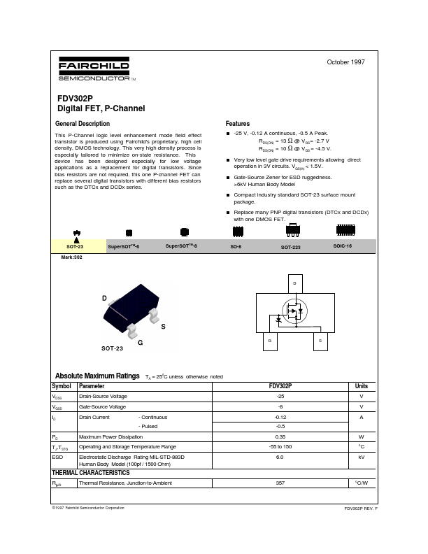
SOT-23 Mark:302
Super SOTTM-6
Super SOTTM-8
SO-8
SOT-223
SOIC-16
Absol...