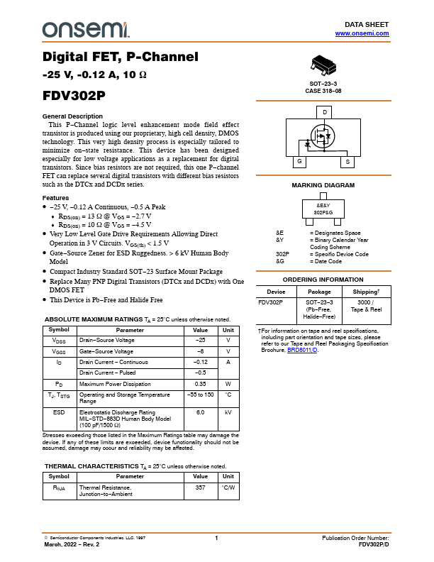
FDV302P
FDV302P is P-Channel Digital FET manufactured by onsemi.
Description
This P- Channel logic level enhancement mode field effect transistor is produced using our proprietary, high cell density, DMOS technology. This very high density process is especially tailored to minimize on- state resistance. This device has been designed especially for low voltage applications as a replacement for digital transistors. Since bias resistors are not required, this one P- channel FET can replace several digital transistors with different bias resistors such as the DTCx and DCDx series.
Features
- - 25 V,
- 0.12 A Continuous,
- 0.5 A Peak
- RDS(on) = 13 W @ VGS =
- 2.7 V
- RDS(on) = 10 W @ VGS =
- 4.5 V
- Very Low Level Gate Drive Requirements Allowing Direct
Operation in 3 V Circuits. VGS(th) < 1.5 V
- Gate- Source Zener for ESD Ruggedness. > 6 k V Human Body
Model
- pact Industry Standard SOT- 23 Surface Mount Package
- Replace Many PNP Digital Transistors (DTCx and DCDx) with One
DMOS FET
- This Device is Pb- Free and Halide Free
ABSOLUTE MAXIMUM RATINGS TA = 25°C unless otherwise noted.
Symbol
Parameter
Value
Unit
VDSS VGSS
Drain- Source Voltage Gate- Source Voltage Drain Current
- Continuous Drain Current
- Pulsed
- 25
- 8
- 0.12
- 0.5
PD TJ, TSTG
Maximum Power Dissipation
Operating and Storage Temperature Range
- 55 to 150...