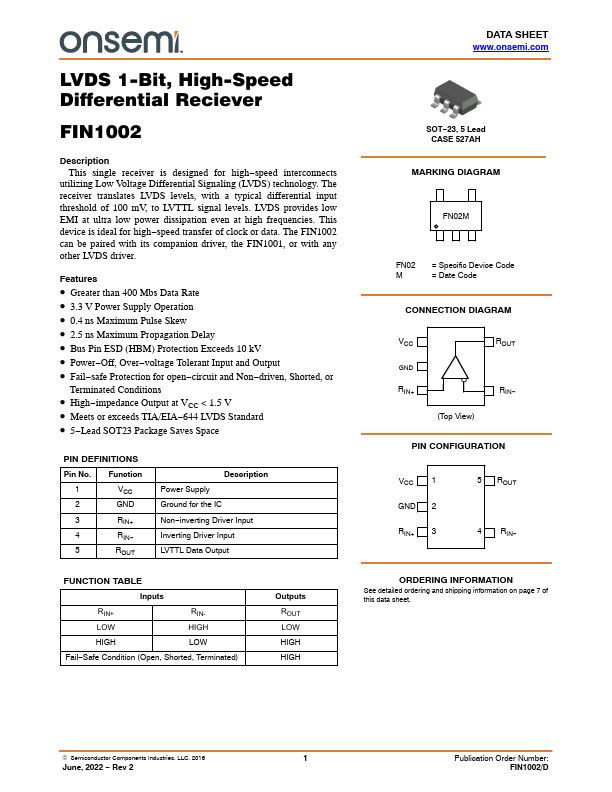
FIN1002
Description
This single receiver is designed for high- speed interconnects utilizing Low Voltage Differential Signaling (LVDS) technology. The receiver translates LVDS levels, with a typical differential input threshold of 100 m V, to LVTTL signal levels. LVDS provides low EMI at ultra low power dissipation even at high frequencies. This device is ideal for high- speed transfer of clock or data. The FIN1002 can be paired with its panion driver, the FIN1001, or with any other LVDS driver.
Features
- Greater than 400 Mbs Data Rate
- 3.3 V Power Supply Operation
- 0.4 ns Maximum Pulse Skew
- 2.5 ns Maximum Propagation Delay
- Bus Pin ESD (HBM) Protection Exceeds 10 k V
- Power- Off, Over- voltage Tolerant Input and Output
- Fail- safe Protection for open- circuit and Non- driven, Shorted, or
Terminated Conditions
- High- impedance Output at VCC < 1.5 V
- Meets or exceeds TIA/EIA- 644 LVDS Standard
- 5- Lead SOT23 Package Saves Space
PIN DEFINITIONS
Pin No. Function
RIN+
RIN-...