Datasheet4U.com
🌙
ISL9V3040D3ST-F085C Datasheet | onsemi
Part:
ISL9V3040D3ST-F085C
Description:
N-Channel IGBT
Manufacturer:
onsemi
Size:
2.41 MB
ISL9V3040D3ST-F085C Datasheet (PDF) Download
onsemi
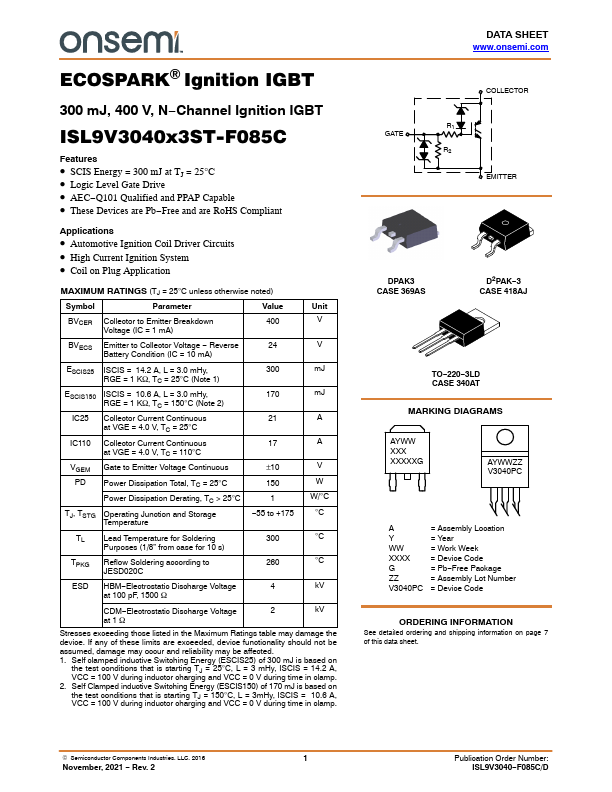
ISL9V3040D3ST-F085C
Key Features
SCIS Energy = 300 mJ at TJ = 25°C
Logic Level Gate Drive
AEC-Q101 Qualified and PPAP Capable
These Devices are Pb-Free and are RoHS compliant
×
Close