Datasheet4U Logo Datasheet4U.com

MC100E111 - 1:9 DIFFERENTIAL CLOCK DRIVER

Description

designed with clock distribution in mind.

It accepts one signal input, which can be either differential or else single-ended if the VBB output is used.

The signal is fanned out to 9 identical differential outputs.

Features

  • Guaranteed Skew Spec.
  • Differential Design.
  • VBB Output.
  • PECL Mode Operating Range: VCC = 4.2 V to 5.7 V with VEE = 0 V.
  • NECL Mode Operating Range: VCC = 0 V with VEE =.
  • 4.2 V to.
  • 5.7 V.
  • Internal Input 50 KW Pulldown Resistors.
  • ESD Protection: > 3 kV Human Body Model.
  • Meets or Exceeds JEDEC Standard EIA/JESD78 IC Latchup Test.
  • Moisture Sensitivity: Level 3 (Pb-Free) (For Additional Information, see Ap.

📥 Download Datasheet

Datasheet preview – MC100E111

Datasheet Details

Part number MC100E111
Manufacturer ON Semiconductor
File Size 155.24 KB
Description 1:9 DIFFERENTIAL CLOCK DRIVER
Datasheet download datasheet MC100E111 Datasheet
Additional preview pages of the MC100E111 datasheet.
Other Datasheets by ON Semiconductor

Full PDF Text Transcription

Click to expand full text
MC10E111, MC100E111 5 V ECL 1:9 Differential Clock Driver Description 
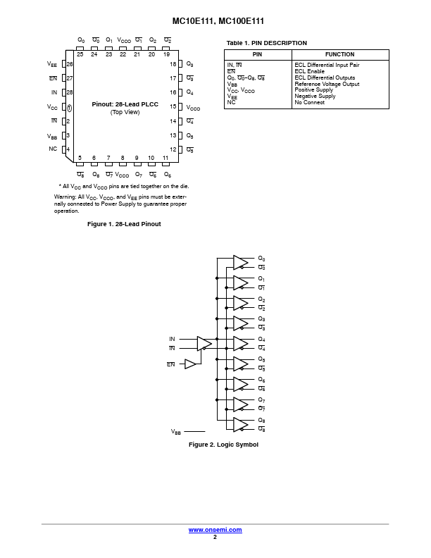
The MC10E/100E111 is a low skew 1-to-9 differential driver, designed with clock distribution in mind. It accepts one signal input, which can be either differential or else single-ended if the VBB output is used. The signal is fanned out to 9 identical differential outputs. An enable input is also provided. A HIGH disables the device by forcing all Q outputs LOW and all Q outputs HIGH. The device is specifically designed, modeled and produced with low skew as the key goal. Optimal design and layout serve to minimize gate to gate skew within-device, and empirical modeling is used to determine process control limits that ensure consistent tpd distributions from lot to lot.
Published: |