Datasheet Details
| Part number | MC100EL14 |
|---|---|
| Manufacturer | onsemi |
| File Size | 137.41 KB |
| Description | 1:5 Clock Distribution Chip |
| Datasheet |
 MC100EL14 Datasheet MC100EL14 Datasheet
|
|
|
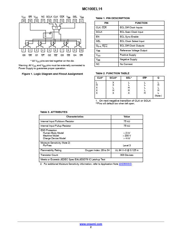
explicitly for low skew clock distribution applications.
The VBB pin, an internally generated voltage supply, is available to this device only.
| Part number | MC100EL14 |
|---|---|
| Manufacturer | onsemi |
| File Size | 137.41 KB |
| Description | 1:5 Clock Distribution Chip |
| Datasheet |
MC100EL14 Datasheet
|
|
|
|