MC100EP51 Key Features
- 350 ps Typical Propagation Delay
- Maximum Frequency > 3 GHz Typical
- PECL Mode Operating Range: VCC = 3.0 V to 5.5 V
- NECL Mode Operating Range: VCC = 0 V
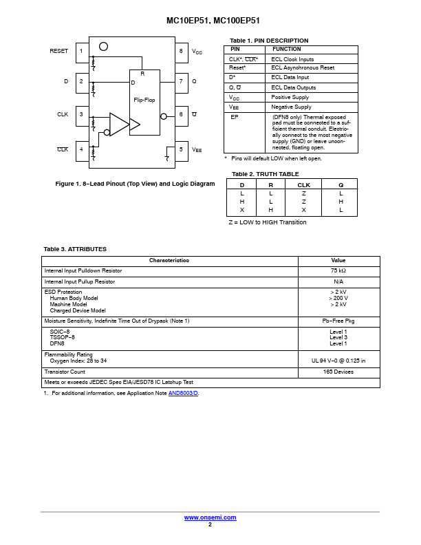
- Open Input Default State
- Safety Clamp on Inputs
- These Devices are Pb-Free and are RoHS pliant
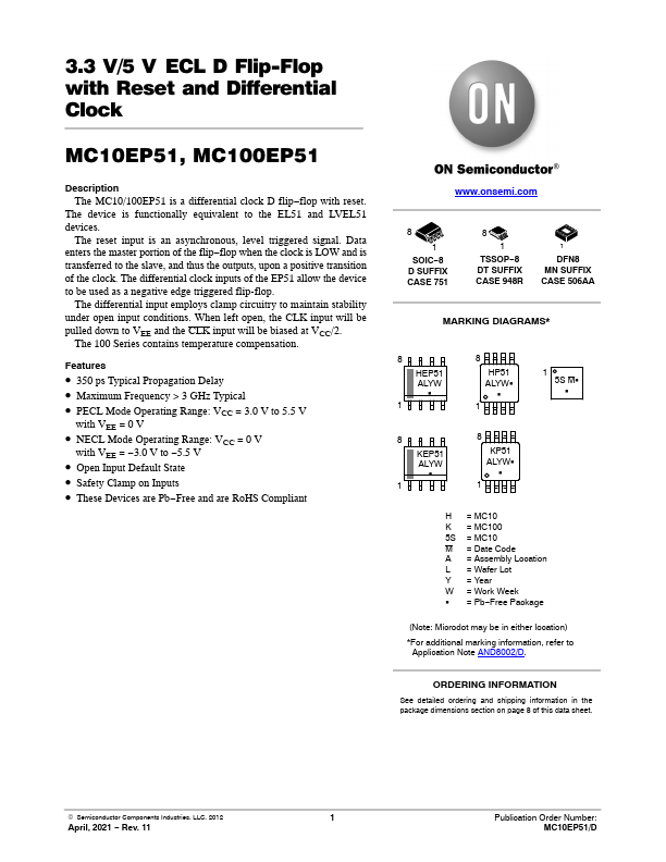
- For additional marking information, refer to Application Note AND8002/D
- Rev. 11
- Pins will default LOW when left open