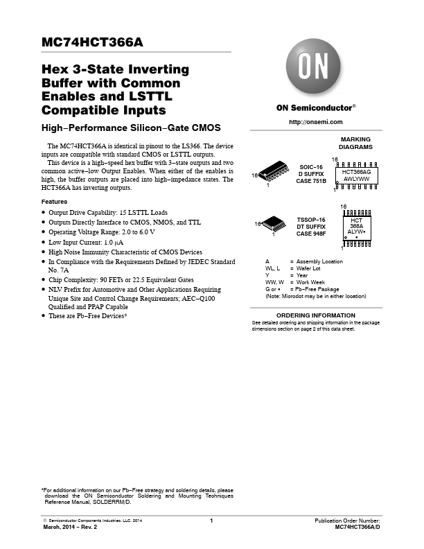
Datasheet4U Logo Datasheet4U.com

MC74HCT366A - Hex 3-State Inverting Buffer

Key Features

  • Output Drive Capability: 15 LSTTL Loads.
  • Outputs Directly Interface to CMOS, NMOS, and TTL.
  • Operating Voltage Range: 2.0 to 6.0 V.
  • Low Input Current: 1.0 mA.
  • High Noise Immunity Characteristic of CMOS Devices.
  • In Compliance with the Requirements Defined by JEDEC Standard No. 7A.
  • Chip Complexity: 90 FETs or 22.5 Equivalent Gates.
  • NLV Prefix for Automotive and Other.

📥 Download Datasheet

Datasheet Details

Part number MC74HCT366A
Manufacturer onsemi
File Size 249.38 KB
Description Hex 3-State Inverting Buffer
Datasheet download datasheet MC74HCT366A Datasheet

Full PDF Text Transcription (Reference)

The following content is an automatically extracted verbatim text from the original manufacturer datasheet and is provided for reference purposes only.

View original datasheet text
MC74HCT366A Hex 3-State Inverting Buffer with Common Enables and LSTTL Compatible Inputs High−Performance Silicon−Gate CMOS The MC74HCT366A is identical in pinout to the LS366. The device inputs are compatible with standard CMOS or LSTTL outputs. This device is a high−speed hex buffer with 3−state outputs and two common active−low Output Enables. When either of the enables is high, the buffer outputs are placed into high−impedance states. The HCT366A has inverting outputs. Features • Output Drive Capability: 15 LSTTL Loads • Outputs Directly Interface to CMOS, NMOS, and TTL • Operating Voltage Range: 2.0 to 6.0 V • Low Input Current: 1.0 mA • High Noise Immunity Characteristic of CMOS Devices • In Compliance with the Requirements Defined by JEDEC Standard No.