MC74VHC1G09
Key Features
- Designed for 2.0 V to 5.5 V VCC Operation
- 4.3 ns tPD at 5 V (typ)
- Inputs/Outputs Over-Voltage Tolerant up to 5.5 V
- IOFF Supports Partial Power Down Protection
- Source/Sink 8 mA at 3.0 V
- Chip plexity < 100 FETs
- Q Suffix for Automotive and Other Applications Requiring Unique Site and Control Change Requirements; AEC-Q100 Qualified and PPAP Capable
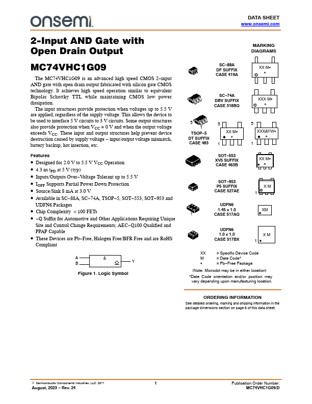
- These Devices are Pb-Free, Halogen Free/BFR Free and are RoHS pliant A & B Y Figure