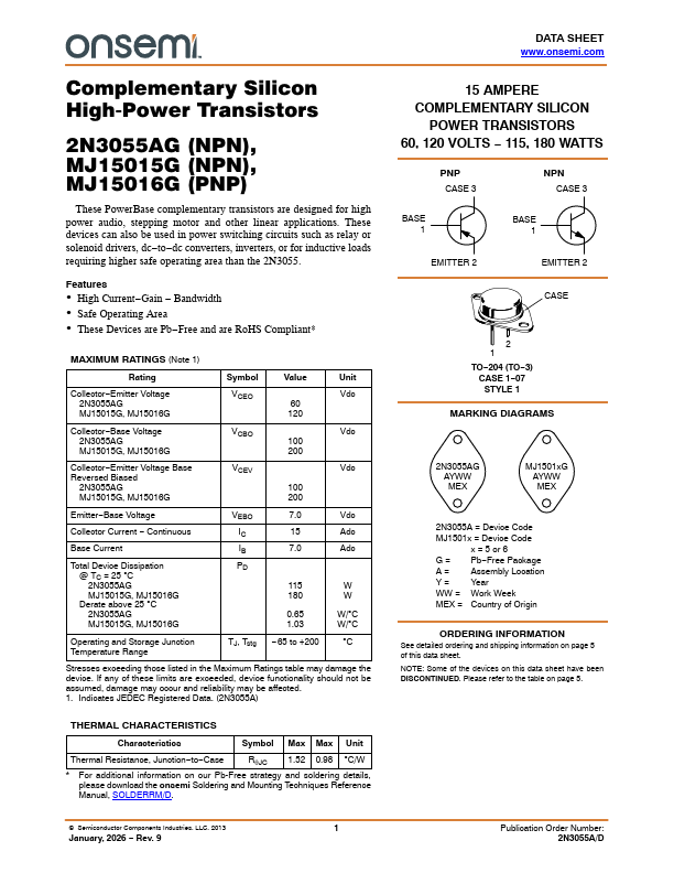
MJ15016G
Features
- High Current- Gain
- Bandwidth
- Safe Operating Area
- These Devices are Pb- Free and are Ro HS pliant-
MAXIMUM RATINGS (Note 1)
Rating
Symbol
Value
Unit
Collector- Emitter Voltage 2N3055AG MJ15015G, MJ15016G
VCEO
Vdc
Collector- Base Voltage 2N3055AG MJ15015G, MJ15016G
VCBO
Vdc
Collector- Emitter Voltage Base Reversed Biased
2N3055AG MJ15015G, MJ15016G
VCEV
Vdc
100 200
Emitter- Base Voltage
Collector Current
- Continuous
Base Current
Total Device Dissipation @ TC = 25 C 2N3055AG MJ15015G, MJ15016G Derate above 25 C 2N3055AG MJ15015G, MJ15016G
VEBO IC IB PD
7.0 15 7.0
115 180 0.65 1.03
Vdc Adc Adc
W W W/C W/C
Operating and Storage Junction Temperature Range
TJ, Tstg
- 65 to +200
C
Stresses exceeding those listed in the Maximum Ratings table may damage the device. If any of these limits are exceeded, device functionality should not be assumed, damage may occur and reliability may be affected. 1. Indicates JEDEC Registered Data....