MMBF4416
Features
- This Device is Designed for RF Amplifiers
- Sourced from Process 50
- This is a Pb- Free and Halide Free Device
ABSOLUTE MAXIMUM RATINGS (TA = 25°C unless otherwise noted.)
Symbol
Parameter
Value
Unit
VDG VGS IGF TJ, TSTG
Drain- Gate Voltage
Gate- Source Voltage
Forward Gate Current
Junction and Storage Temperature Range
- 30
10 m A
- 55 to +150 _C
Stresses exceeding those listed in the Maximum Ratings table may damage the device. If any of these limits are exceeded, device functionality should not be assumed, damage may occur and reliability may be affected.
THERMAL CHARACTERISTICS (TA = 25°C unless otherwise noted.) (Note 1)
Symbol
Parameter
Total Device Dissipation Derate above
25_C
Rq JA Thermal Resistance, Junction to Ambient 1. Device mounted on FR- 4 PCB 1.6″ × 1.6″ × 0.06″.
Max
Unit
225 m W
1.8 m W/_C
°C/W
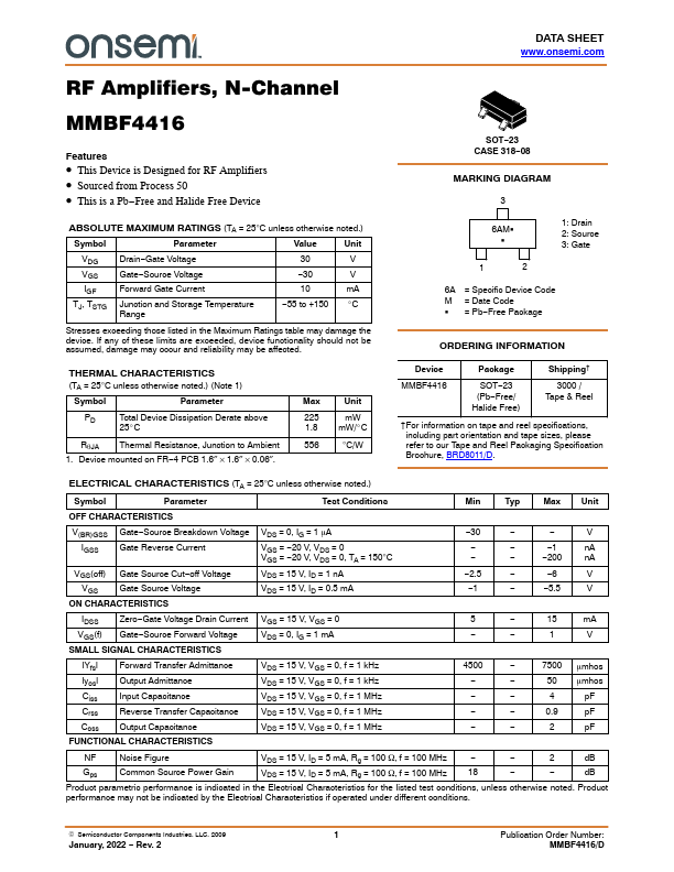
SOT- 23 CASE 318- 08
MARKING DIAGRAM
6AMG G
1: Drain 2: Source 3:...