Click to expand full text
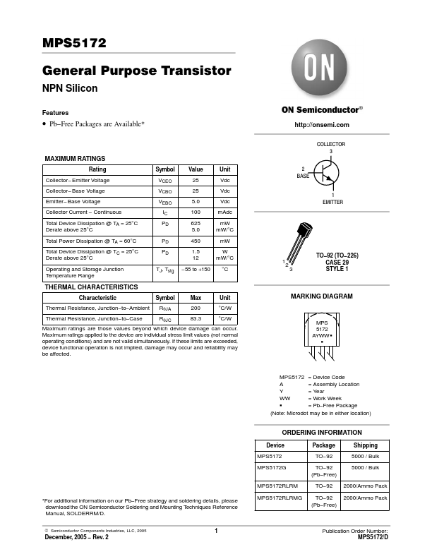
MPS5172
General Purpose Transistor
NPN Silicon
Features
• Pb−Free Packages are Available*
MAXIMUM RATINGS
Rating Collector−Emitter Voltage Collector−Base Voltage Emitter−Base Voltage Collector Current − Continuous Total Device Dissipation @ TA = 25°C Derate above 25°C
Symbol VCEO VCBO VEBO
IC PD
Value 25 25 5.0 100 625 5.0
Unit Vdc Vdc
Vdc
mAdc
mW mW/°C
Total Power Dissipation @ TA = 60°C Total Device Dissipation @ TC = 25°C Derate above 25°C
PD 450 mW PD 1.5 W
12 mW/°C
Operating and Storage Junction Temperature Range
TJ, Tstg −55 to +150 °C
THERMAL CHARACTERISTICS
Characteristic
Symbol
Max
Unit
Thermal Resistance, Junction−to−Ambient RqJA
200 °C/W
Thermal Resistance, Junction−to−Case
RqJC
83.3 °C/W
Maximum ratings are those values beyond which device damage can occur.