MTB3N100E Overview
Key Specifications
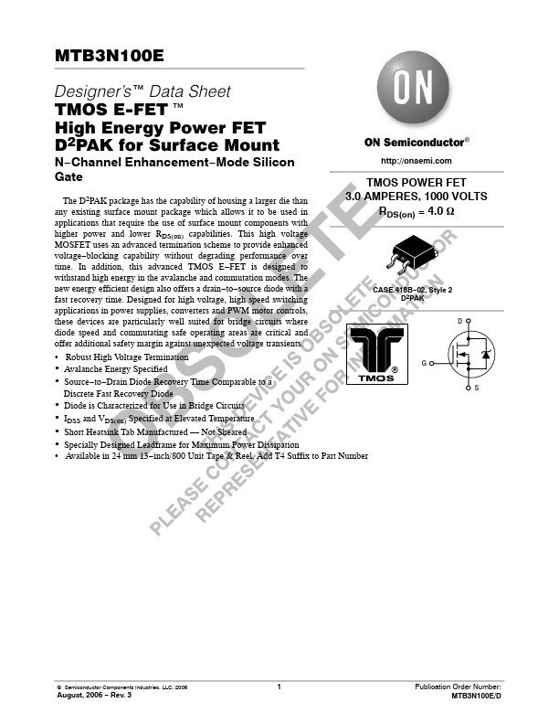
Package: D2PAK
Mount Type: Surface Mount
Pins: 3
Max Operating Temp: 150 °C
Key Features
- Robust High Voltage Termination
- Avalanche Energy Specified
| Part | MTB3N100E |
|---|---|
| Description | High Energy Power FET |
| Manufacturer | onsemi |
| Size | 276.02 KB |
Package: D2PAK
Mount Type: Surface Mount
Pins: 3
Max Operating Temp: 150 °C
| Seller | Inventory | Price Breaks | Buy |
|---|---|---|---|
| Win Source | 5 | 10+ : 5.1732 USD 24+ : 4.2447 USD 37+ : 4.1121 USD 51+ : 3.9794 USD |
View Offer |
| Part Number | Manufacturer | Description |
|---|---|---|
| 3N100E | Motorola Semiconductor | MTB3N100E |
| MTB3N100E | Motorola Semiconductor | TMOS POWER FET |