N04L63W2A
N04L63W2A is 4Mb Ultra-Low Power Asynchronous CMOS SRAM manufactured by onsemi.
Overview
The N04L63W2A is an integrated memory device containing a 4 Mbit Static Random Access Memory organized as 262,144 words by 16 bits. The device is designed and fabricated using ON Semiconductor’s advanced CMOS technology to provide both high-speed performance and ultra-low power. The device operates with two chip enable (CE1 and CE2) controls and output enable (OE) to allow for easy memory expansion. Byte controls (UB and LB) allow the upper and lower bytes to be accessed independently and can also be used to deselect the device. The N04L63W2A is optimal for various applications where low-power is critical such as battery backup and hand-held devices. The device can operate over a very wide temperature range of -40o C to +85o C and is available in JEDEC standard packages patible with other standard 256Kb x 16 SRAMs
..
Features
- Single Wide Power Supply Range 2.3 to 3.6 Volts
- Very low standby current 4.0µA at 3.0V (Typical)
- Very low operating current 2.0m A at 3.0V and 1µs (Typical)
- Very low Page Mode operating current 0.8m A at 3.0V and 1µs (Typical)
- Simple memory control Dual Chip Enables (CE1 and CE2) Output Enable (OE) for memory expansion
- Low voltage data retention Vcc = 1.8V
- Very fast output enable access time 25ns OE access time
- Automatic power down to standby mode
- TTL patible three-state output driver
- pact space saving BGA package available
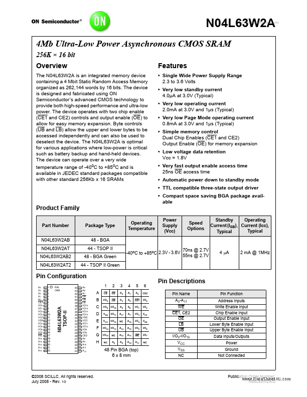
Product Family
Part Number N04L63W2AB N04L63W2AT N04L63W2AB2 N04L63W2AT2 Package Type 48
- BGA 44
- TSOP II 48
- BGA Green 44
- TSOP II Green 70ns @ 2.7V -40o C to +85o C 2.3V
- 3.6V 55ns @ 2.7V 4 µA 2 m A @ 1MHz Operating Temperature Power Supply (Vcc) Speed Options Standby Operating Current (ISB), Current (Icc), Typical Typical
Pin Configuration
A4 A3 A2 A1 A0 CE1 I/O0 I/O1 I/O2 I/O3 VCC VSS I/O4 I/O5 I/O6 I/O7 WE A16 A15 A14 A13 A12 1 2 3 4 5 6 7 8 9 10 11 12 13 14 15 16 17 18 19 20 21 22 PIN ONE 44 43 42 41 40 39 38 37 36 35 34 33 32 31 30 29 28 27 26 25 24 23 A5 A6 A7 OE UB LB I/O15 I/O14...