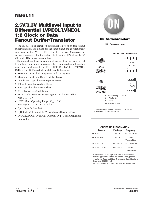
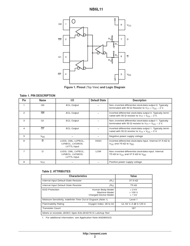
Datasheet4U Logo Datasheet4U.com

NB6L11 - 2.5V / 3.3V MULTILEVEL INPUT TO DIFFERENTIAL LVPECL/LVNECL

Description

Pin 1 2 3 4 5 6 Name Q0 Q0 Q1 Q1 VEE D ÁÁÁÁ ÁÁÁÁÁÁ ÁÁÁÁÁÁÁÁ ÁÁÁÁ ÁÁÁÁÁÁ ÁÁÁÁÁÁÁÁ ÁÁÁÁ ÁÁÁÁÁÁ ÁÁÁÁÁÁÁÁ I/O ECL Output ECL Output ECL Output ECL Output LVDS, CML, LVPECL, LVNECL, LVCMOS, LVTTL Input LVDS, CML, LVPECL, LVNECL, LVCMOS, LVTTL Input Default State

Features

  • ttp://onsemi. com 5 NB6L11 Table 6. DC.

📥 Download Datasheet

Datasheet preview – NB6L11

Datasheet Details

Part number NB6L11
Manufacturer onsemi
File Size 114.83 KB
Description 2.5V / 3.3V MULTILEVEL INPUT TO DIFFERENTIAL LVPECL/LVNECL
Datasheet download datasheet NB6L11 Datasheet
Additional preview pages of the NB6L11 datasheet.
Other Datasheets by ON Semiconductor

Full PDF Text Transcription

Click to expand full text
NB6L11 2.5V/3.3V Multilevel Input to Differential LVPECL/LVNECL 1:2 Clock or Data Fanout Buffer/Translator The NB6L11 is an enhanced differential 1:2 clock or data fanout buffer/translator. The device has the same pinout and is functionally equivalent to the LVEL11, EP11, LVEP11 devices. Moreover, the device is optimized for the systems that require LOW skew, LOW jitter and LOW power consumption. Differential input can be configured to accept single−ended signal by applying an external reference voltage to unused complimentary input pin. Input accept LVNECL, LVPECL, LVTTL, LVCMOS, CML, or LVDS. The outputs are 800 mV ECL signals.
Published: |